Understanding FR-4 Material in PCB Design
If you are new to printed circuit board (PCB) design and planning to create your initial board using FR-4 material, this guide is an ideal starting point. It will navigate you through the core aspects of FR-4 PCB design for beginners, encompassing everything from comprehending the material's properties to designing both single-layer and double-layer boards with widely used software tools. This step-by-step tutorial offers actionable insights to help you commence your design journey.
This comprehensive article will deeply explore the process of designing with PCB FR4 material, which is the most common material utilized for printed circuit boards globally. You will grasp the foundational principles of PCB design with FR-4, discover various software options, and follow detailed instructions for crafting both single-layer and double-layer designs.

What Exactly Is FR-4?
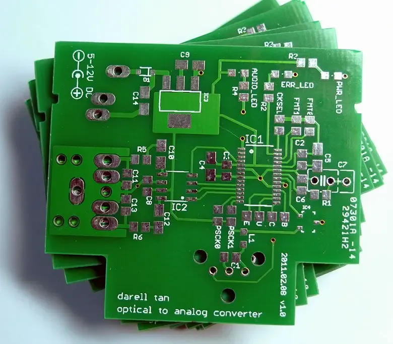
FR-4 is a specific type of fiberglass-reinforced epoxy laminate that functions as the foundational material for the majority of printed circuit boards. The "FR" abbreviation denotes "Flame Retardant," indicating its inherent fire-resistant properties, which makes it a secure choice for diverse electronic applications. Its widespread adoption stems from its balanced combination of affordability, robust durability, and effective electrical insulation characteristics, rendering it suitable for both novice designers and seasoned professionals.
FR-4 possesses a dielectric constant of approximately 4.5, which is well-suited for a broad spectrum of low to medium-frequency applications. It also provides commendable mechanical strength, ensuring that your PCB can withstand physical stresses during both assembly and operational use. For hobbyists and engineers working on either single-layer or double-layer FR-4 PCB designs, this material is frequently the preferred option due to its lower circuit board cost and versatile applications.
Related Reading: Exploring the World of Multilayer FR-4 PCBs: Design, Manufacturing, and Applications
Initial Steps for FR-4 PCB Design: Tools and Preparation
Before delving into the actual design phase, it is essential to assemble the appropriate tools and prepare your work environment. The primary step involves selecting the right FR-4 PCB design software that aligns with your current skill level and project specific requirements. Below are three highly recommended options suitable for beginners:
Popular Design Software for Beginners
● Eagle: This tool is known for its user-friendly interface, extensive community support, and vast component libraries, making it an excellent starting point for learning FR-4 PCB design.
● KiCad: As a free, open-source software suite, KiCad is an ideal choice for hobbyists and students, offering a comprehensive set of features for schematic capture and PCB layout.
● Altium Designer: Representing a professional-grade solution, Altium Designer is geared towards more intricate designs, providing advanced functionalities for complex PCB development.
Beyond software, you will also need a fundamental understanding of your project’s requirements. This includes defining the circuit's intended function, identifying all necessary components, and determining whether a single-layer or double-layer board will best suit your needs. Single-layer boards are simpler to design and typically less expensive, whereas double-layer boards accommodate more complex circuits and offer superior signal routing capabilities.
Step-by-Step Tutorial for FR-4 PCB Design
With your tools ready, let's proceed with the process of designing a PCB using FR-4 material. This guide covers both single-layer and double-layer FR-4 PCB designs, with specific distinctions highlighted where applicable.
Step 1: Define Your Circuit Requirements
Begin by meticulously outlining the functional requirements of your circuit. Compile a comprehensive list of all components, such as resistors, capacitors, and microcontrollers, along with their precise specifications. For example, if designing a straightforward LED circuit, note the required voltage (e.g., 5V) and current draw (e.g., 20mA per LED). This foundational step ensures that your final board design will precisely meet your project's electrical and physical demands.
Step 2: Create a Schematic Diagram
Using your chosen PCB design software, construct a schematic diagram that visually represents your circuit. This diagram serves as an electrical blueprint, illustrating how all components are interconnected. In software environments like KiCad or Eagle, you can easily drag and drop components from their respective libraries and establish connections using virtual wires. Verifying the accuracy of all connections at this stage is crucial to prevent significant issues later in the PCB design process. For beginners using KiCad, start by opening the schematic editor, adding components, and clearly labeling nets for enhanced clarity. In Eagle, the procedure is similar, with an emphasis on selecting appropriate library parts. Altium Designer provides more sophisticated features, including real-time error checking, which can proactively identify mistakes.
Step 3: Design the PCB Layout
Once your schematic is finalized, transition to the PCB layout editor within your software. This phase involves arranging components physically on the FR-4 board and routing the copper traces that electrically connect them. For a single-layer FR-4 PCB design, all traces must be confined to one side of the board. In contrast, for a double-layer FR-4 PCB design, you have the flexibility to utilize both sides, which permits shorter traces and inherently reduces electromagnetic interference.
Keep the following tips in mind during the layout phase:
● Place components logically, grouping related parts together to minimize trace lengths.
● On single-layer boards, endeavor to avoid crossing traces; use jumpers if absolutely necessary.
● For double-layer designs, employ vias (small plated holes) to establish connections between layers.
● Maintain an appropriate trace width that can safely carry the required current. For example, a trace conducting 1A might need a width of 0.5mm on 1oz copper FR-4 material.
Step 4: Set Design Rules Specific to FR-4 Material
FR-4's specific material properties directly influence the design rules you must adhere to, particularly concerning impedance and thermal management. Most PCB design software tools allow you to configure constraints such as minimum trace width (e.g., 0.2mm for standard designs) and clearance (e.g., 0.2mm between adjacent traces) to ensure manufacturability. Given FR-4's dielectric constant of approximately 4.5, which affects signal speed, it is advisable to keep traces short when working with high-frequency designs (above 100MHz). In Altium, these parameters are configured within the design rule editor. Eagle and KiCad offer similar functionalities, typically found in their settings or constraints menus, making them accessible.
Step 5: Route Traces and Optimize Layout
Routing involves drawing the copper traces that establish the electrical connections between components. For a single-layer board, this can be quite challenging due to inherent space limitations, thus requiring meticulous planning. Double-layer boards offer considerably more flexibility, as you can route power and ground planes on separate layers to effectively reduce noise and improve signal integrity.
Pay close attention to signal integrity during routing. For instance, ensure that high-speed signals (above 50MHz) are kept sufficiently isolated from power lines to prevent undesirable interference. Furthermore, utilizing a solid ground plane on one layer of a double-layer board can significantly enhance stability and reduce electromagnetic interference (EMI).
Related Reading: The Ultimate Guide to Connecting Components with Inner Layer Traces
Step 6: Verify and Export Your Design
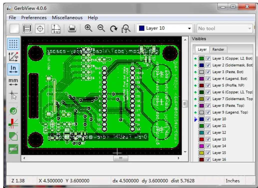
Before submitting your design for manufacturing, it is imperative to conduct a comprehensive Design Rule Check (DRC) using your software. This check identifies potential errors such as unconnected pins or overlapping traces. Most tools like KiCad, Eagle, and Altium have integrated DRC features that highlight issues visually or through error messages. Once the design is thoroughly verified and error-free, export your design files, typically in Gerber format, which is the industry standard for PCB manufacturing. Ensure that your export settings include all necessary layers for copper, solder mask, and silkscreen.
Single-Layer vs. Double-Layer FR-4 PCB Design: Key Distinctions
The decision between a single-layer FR-4 PCB design and a double-layer FR-4 PCB design largely depends on the complexity of your project. Here’s a concise comparison:
● Single-Layer: Best suited for simple circuits with fewer components. These boards are typically cheaper to manufacture and easier to design, though they offer limited routing options. They are ideal for basic projects such as LED drivers or simple power distribution boards.
● Double-Layer: Recommended for more complex circuits featuring higher component densities. Double-layer boards provide enhanced signal routing capabilities and allow for the implementation of dedicated ground planes, which effectively reduces noise. They are perfect for microcontroller-based designs or projects with multiple integrated circuits.
For beginners, it is often advisable to start with a single-layer board to firmly grasp the fundamentals of basic FR-4 PCB design before progressing to more intricate double-layer designs.
Selecting the Appropriate FR-4 PCB Design Software
Your choice of FR-4 PCB design software can profoundly influence your learning trajectory and the ultimate quality of your designs. Here’s a detailed breakdown of the three tools previously mentioned, specifically tailored for beginners:
Software Options for FR-4 PCB Design
● Eagle for FR-4 PCB Design: Eagle is well-regarded for its intuitive user interface and extensive component libraries, making it an excellent starting point. It fully supports both single and double-layer designs with user-friendly schematic and layout editors. Its free version is typically sufficient for smaller projects that require up to two signal layers.
● KiCad for FR-4 PCB Design: KiCad is a powerful, free, and open-source tool that rivals commercial software. It offers a complete suite for schematic capture, PCB layout, and even sophisticated 3D visualization of your FR-4 board. Its open-source nature ensures continuous updates and strong community support, making it an excellent choice for a wide range of projects.
● Altium Designer for FR-4 PCB Design: Altium Designer stands as a premium option, primarily targeting professionals and advanced hobbyists. It excels in managing complex double-layer designs, offering advanced features such as interactive routing and precise impedance control for high-speed signals on FR-4 material. While it does present a steeper learning curve, its capabilities for professional-grade design are unparalleled.
Practical Tips for Successful FR-4 PCB Design
To conclude, here are some practical tips to ensure your FR-4 PCB design journey is smooth and productive:
● Begin with Simplicity: Always start with small, uncomplicated projects to progressively build confidence in basic FR-4 PCB design principles.
● Verify Component Footprints: Consistently double-check component footprints against their respective datasheets to prevent sizing errors during layout.
● Utilize Ground Planes: For double-layer designs, always incorporate a solid ground plane to effectively minimize noise and enhance signal integrity.
● Shorten Trace Lengths for High Frequencies: Keep trace lengths as short as possible for high-frequency signals to avoid delays, taking into account FR-4’s dielectric constant of 4.5.
● Simulate When Possible: If your chosen software, like Altium, offers built-in simulation tools, utilize them to predict and optimize the performance of your design before fabrication.
Conclusion: Embark on Your FR-4 PCB Design Journey Today
Designing a PCB using FR-4 material is an exciting and entirely achievable endeavor, even for those new to the field. By following this detailed step-by-step tutorial, you have acquired fundamental knowledge concerning both single-layer and double-layer FR-4 PCB design, along with practical guidance on utilizing popular FR-4 PCB design software such as Eagle, KiCad, and Altium. From creating precise schematics to routing efficient traces and exporting manufacturing files, you now possess the essential foundation to transform your electronic concepts into tangible reality.
Whether you are a hobbyist exploring new interests or an aspiring engineer building your portfolio, FR-4 provides a reliable and cost-effective base for a vast array of projects. Select a software tool that suits your needs, commence with a simple design, and gradually tackle more complex boards as your experience grows. With diligent practice, you will master basic FR-4 PCB design and beyond, enabling you to create innovative circuits that power groundbreaking solutions.


