Introduction
Printed circuit boards form the backbone of modern electronics, enabling everything from consumer devices to industrial controls. As electrical engineers push for higher performance and miniaturization, the environmental footprint of PCB materials has come under scrutiny. The phrase "cradle to grave" refers to the full life cycle assessment of these materials, from raw resource extraction through manufacturing, use, and disposal. This holistic view reveals significant challenges, particularly with dominant substrates like FR-4, whose production and end-of-life handling contribute to resource depletion and waste accumulation. Engineers must now integrate sustainability into material selection PCB processes to meet regulatory pressures and corporate goals. Understanding the environmental impact of FR-4 and exploring alternative PCB substrates can guide designs toward lower ecological harm while maintaining reliability.
In PCB manufacturing facilities, the focus has shifted toward traceable supply chains and reduced emissions. Traditional materials rely on non-renewable resources, leading to high energy demands and chemical releases. Biodegradable PCB materials and eco-friendly PCB laminates emerge as promising shifts, but they require rigorous qualification. This article dissects these impacts stage by stage, offering factory-driven insights for engineers balancing performance with planetary responsibility.
The Life Cycle of PCB Materials: Cradle to Grave
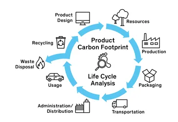
Life cycle assessment provides a standardized framework to quantify environmental burdens across all phases of a PCB's existence. Raw material extraction begins with mining silica for glass fibers, petroleum-based epoxy resins, and copper ores, each process consuming vast energy and generating tailings. Manufacturing involves layering these into laminates, etching circuits, and applying finishes, often under high heat and pressure that emit volatile organic compounds. During the use phase, PCBs endure thermal cycling and mechanical stress, but their durability minimizes frequent replacements.
End-of-life poses the greatest challenge, as composite structures resist breakdown, leading to e-waste accumulation in landfills or incineration that releases toxins. Factory insights reveal that improper handling amplifies soil and water contamination from heavy metals. Engineers applying life cycle thinking early in design can prioritize recyclable components. This approach aligns with broader industry efforts to extend material lifespans and recover valuables like copper.
Global electronics production exacerbates these issues, with PCBs comprising a significant portion of e-waste. Assessing each stage uncovers hotspots, such as resin curing's carbon footprint. Proactive evaluation informs scalable improvements in production lines.
Environmental Impact of FR-4: A Dominant Substrate Under Scrutiny
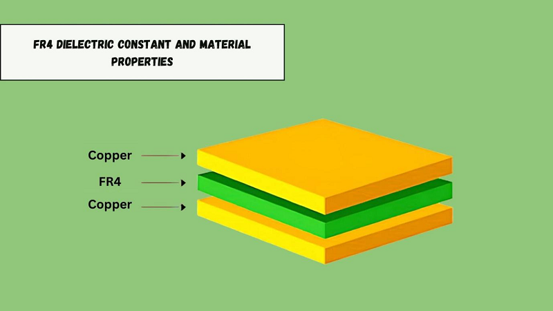
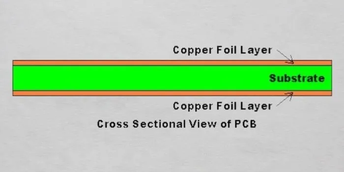
FR-4, the most prevalent PCB laminate, consists of woven E-glass fabric impregnated with brominated epoxy resin for flame retardancy. Its environmental impact of FR-4 spans the entire life cycle, starting with resin synthesis from fossil fuels, which drives high greenhouse gas emissions. Glass fiber production requires melting silica at over 1400 degrees Celsius, consuming substantial electricity often from non-renewable sources. During fabrication, brominated compounds pose risks if released, as they persist in ecosystems.
In the use phase, FR-4 excels with stable dielectric properties and high glass transition temperatures, supporting reliable operation. However, disposal reveals vulnerabilities: the material does not biodegrade, and mechanical recycling shreds it into unusable fibers mixed with resins. Incineration can liberate halogens, forming dioxins under incomplete combustion. Factories report challenges in separating layers for material recovery, leading to downcycling or landfilling.
Standards like IPC-4101B guide FR-4 qualification, specifying properties such as flammability per UL 94 V-0, yet they do not directly address life cycle burdens. Engineers note that while FR-4 meets performance needs, its cumulative impact demands alternatives for volume production. Cumulative data from production scales highlight raw materials as the largest contributor to overall footprint.
Challenges in Recycling Traditional PCB Materials
Recycling PCBs involves dismantling to recover copper, gold, and tin, but FR-4 substrates complicate processes due to their thermoset nature. Pyrolysis or hydrometallurgy extracts metals, yet resins leave hazardous residues requiring treatment. Factory lines optimized for high-volume FR-4 struggle with variability in e-waste streams, reducing yield rates. Contaminants from solders and coatings further degrade recyclate quality.
Landfill disposal buries non-degradable composites, leaching additives over decades. Incineration for energy recovery risks air pollution without advanced scrubbers. Engineers face trade-offs: robust designs extend life but hinder disassembly. Comprehensive strategies demand design-for-recyclability from inception.
Emerging pyrometallurgical methods show promise, but scalability lags. Insights from production floors emphasize preprocessing like shredding and eddy current separation. Despite efforts, recovery rates hover below optimal, underscoring the need for material innovation.
Alternative PCB Substrates: Pathways to Reduced Impact
Alternative PCB substrates address FR-4's limitations by incorporating renewable fibers or thermoplastic matrices. Halogen-free laminates replace brominated resins with phosphorus-based retardants, minimizing toxic releases during fires or disposal. Paper-phenolic composites, akin to CEM-1, use cellulose reinforcements for lower density and easier pulping. These options align with factory shifts toward cleaner chemistries.
Polyimide films offer flexibility but at higher costs; bio-derived versions from plant oils reduce petroleum dependence. Lignocellulosic nanofibrils from wood provide high strength with biodegradability potential. Selection criteria include thermal stability, moisture absorption, and CTE matching to copper.
In practice, these substrates demand requalification per IPC standards to ensure solder joint integrity. Production trials reveal adjusted press cycles for optimal bonding. Engineers benefit from hybrid stacks combining FR-4 cores with green outer layers.
Eco-Friendly and Biodegradable PCB Materials: Emerging Factory Realities
Eco-friendly PCB laminates prioritize low-VOC resins and recycled glass content, easing manufacturing emissions. Biodegradable PCB materials, such as polylactic acid composites or mycelium-inspired matrices, decompose under composting conditions. Derived from corn starch or agricultural waste, they target transient applications like sensors. Factory validation tests hydrolysis rates and fungal resistance.
These materials exhibit dielectric constants suitable for low-frequency boards, with ongoing refinements for high-speed signals. Challenges include lower Tg limiting reflow soldering, addressed via fillers. ISO 14001 frameworks guide factories in auditing these innovations for verifiable reductions.
Deployment in prototypes demonstrates viability, with disposal yielding compostable remnants. Scalability hinges on supply chain maturity. Engineers integrate them via iterative testing, balancing eco-gains with reliability.
Best Practices for Material Selection in Sustainable PCB Design
Material selection PCB starts with defining environmental priorities alongside electrical and thermal specs. Catalog specs per IPC-4101B inform choices like dielectric thickness and peel strength. Prioritize halogen-free grades for compliance and recyclability. Simulate life cycle hotspots using simplified models focused on energy and waste.
Collaborate with fabricators early to validate prototypes under real conditions. Opt for modular designs facilitating component harvest. Track metrics like embodied carbon through supplier declarations.
Factory best practices include solvent-free processes and energy-efficient curing. ISO 14001 certification ensures systematic improvements. Engineers document trade-offs in design reviews for informed decisions.
Conclusion
Analyzing PCB materials from cradle to grave exposes FR-4's substantial environmental toll through resource intensity and disposal hurdles. Alternative PCB substrates, eco-friendly PCB laminates, and biodegradable PCB materials offer tangible paths forward, demanding careful integration. Factory-driven approaches, guided by standards, empower engineers to select materials that sustain performance without compromising the planet. Prioritizing life cycle thinking in design yields resilient, greener electronics. As production evolves, these choices will define the industry's legacy.
FAQs
Q1: What is the primary environmental impact of FR-4 in PCB manufacturing?
A1: FR-4's reliance on petroleum-based epoxies and glass fibers drives high energy use and emissions during synthesis and curing. Brominated flame retardants complicate end-of-life treatment, as they persist in waste streams. Factories mitigate via halogen-free variants, but full impacts span extraction to disposal. Engineers assess via life cycle stages for targeted reductions.
Q2: How do alternative PCB substrates compare to FR-4 environmentally?
A2: Alternative PCB substrates like cellulose-reinforced laminates lower raw material footprints by using renewables, easing recycling. They reduce incineration risks without halogens. Qualification per IPC standards ensures compatibility. Factory insights favor them for low-volume, eco-focused runs.
Q3: Are biodegradable PCB materials ready for production-scale use?
A3: Biodegradable PCB materials suit disposable electronics, decomposing naturally post-use. Challenges include thermal limits, addressed through reinforcements. ISO 14001 aids factory adoption. They promise e-waste cuts but require performance validation.
Q4: What role does material selection play in PCB sustainability?
A4: Material selection PCB integrates eco-metrics early, balancing cost, reliability, and impact. Prioritize specs like biodegradability for targeted apps. Collaborate across design and fab for optimized stacks.
References
IPC-4101B — Specification for Base Materials for Rigid and Multilayer Printed Boards. IPC, 2006
ISO 14001:2015 — Environmental Management Systems. ISO, 2015