Introduction
High Density Interconnect (HDI) PCB design for 5G applications represents a pivotal advancement in modern electronics, addressing the stringent demands of high speed data transmission and compact form factors. As 5G technology rolls out globally, it requires printed circuit boards capable of supporting high frequency signals, low signal loss, and dense component integration. HDI PCBs, with their fine traces, microvias, and multilayer structures, are uniquely suited to meet these challenges. This article explores the critical aspects of 5G PCB design, focusing on high frequency HDI PCB considerations. Aimed at electrical engineers, the content delves into technical principles, best practices, and industry standards to ensure optimal performance in next generation communication systems. Understanding these elements is essential for designing reliable and efficient solutions in this rapidly evolving field.
What Is HDI PCB Design and Why It Matters for 5G
HDI PCB design refers to a technology that enables higher component density and finer interconnects on printed circuit boards through the use of microvias, blind vias, and buried vias. Unlike traditional PCBs, HDI boards incorporate smaller geometries and multiple layers, allowing for compact layouts essential in modern electronics. For 5G applications, this technology is critical due to the need for high frequency signal transmission, often in the range of several gigahertz, and minimal signal interference.
The importance of HDI PCB design for 5G lies in its ability to support the dense integration of components required for advanced radio frequency modules and baseband processing units. With 5G networks demanding faster data rates and lower latency, high frequency HDI PCBs ensure signal integrity and efficient power distribution. This capability directly impacts the performance of devices such as smartphones, IoT systems, and base stations, making HDI a cornerstone of 5G infrastructure.
Technical Principles of High Frequency HDI PCB Design
Designing HDI PCBs for 5G applications involves understanding several core technical principles related to high frequency signal behavior and board architecture. At high frequencies, signal propagation is affected by factors such as dielectric loss, skin effect, and impedance mismatches. These phenomena necessitate precise control over trace width, spacing, and dielectric material properties to minimize signal degradation.
One key principle is impedance control, which ensures consistent signal transmission across the board. For 5G systems operating at millimeter wave frequencies, maintaining a specific characteristic impedance is vital to avoid reflections. This requires careful selection of substrate materials with low dielectric constants and loss tangents, as well as precise trace geometries.
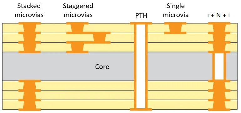
Another critical aspect is the use of microvias in HDI designs. These small diameter vias, often less than 0.15 millimeters, enable high density routing between layers without occupying excessive board space. Their placement and aspect ratio must be optimized to prevent signal distortion and ensure reliability under thermal stress.
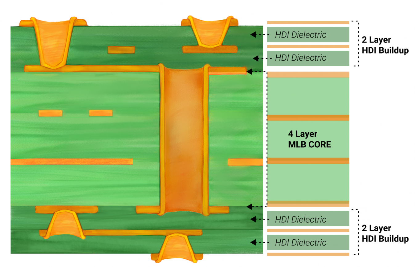
Electromagnetic interference also poses a challenge in high frequency HDI PCB design. Proper grounding techniques and shielding layers are necessary to mitigate crosstalk between adjacent traces. Additionally, stackup configuration plays a significant role, with symmetrical layer arrangements helping to reduce warpage and maintain signal integrity.
Material Selection for 5G PCB Design
Material choice is a foundational element in high frequency HDI PCB design for 5G. At elevated frequencies, the dielectric properties of the substrate directly influence signal loss and propagation speed. Materials with low dielectric constants and minimal loss tangents are preferred to reduce attenuation and maintain signal clarity over long traces.
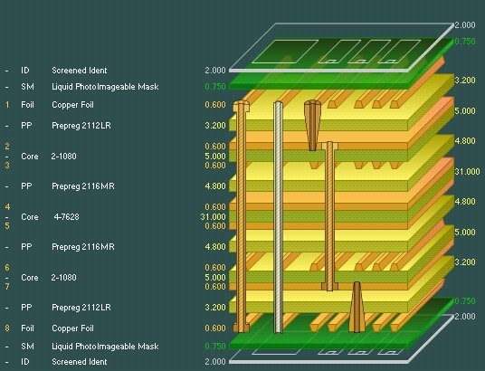
Commonly used materials for high frequency applications must comply with industry standards for thermal stability and electrical performance. The selection process also considers the coefficient of thermal expansion to ensure compatibility between layers during temperature fluctuations. This prevents delamination and maintains structural integrity in demanding 5G environments.
Beyond electrical properties, mechanical characteristics such as rigidity and moisture absorption are evaluated to guarantee long term reliability. For multilayer HDI designs, the bonding materials between layers must withstand the thermal cycles encountered during manufacturing and operation. Adhering to recognized standards ensures that the chosen materials meet the rigorous demands of 5G technology.
Best Practices for HDI PCB Design in 5G Applications
Implementing best practices in HDI PCB design for 5G applications optimizes performance and manufacturability. Engineers must prioritize several strategies to address the unique challenges of high frequency environments.
First, meticulous stackup planning is essential. A balanced stackup with alternating signal and ground layers minimizes electromagnetic interference and supports controlled impedance. Ground planes should be continuous where possible to provide a stable reference for high frequency signals.
Second, via design requires careful attention. Microvias should be strategically placed to shorten signal paths and reduce parasitic inductance. Blind and buried vias can be utilized to free up surface space for component placement, but their aspect ratios must align with manufacturing capabilities to avoid reliability issues.
Third, trace routing must account for signal integrity. Differential pairs, common in 5G designs for data transmission, need matched lengths and consistent spacing to prevent skew. Corners in traces should use smooth curves rather than sharp angles to minimize signal reflections at high frequencies.
Thermal management is another critical consideration. High density designs generate significant heat, particularly in 5G devices with power intensive components. Incorporating thermal vias and heat dissipation layers helps maintain operational temperatures within safe limits, preserving component lifespan.
Finally, adherence to industry standards such as IPC-2226, which provides guidelines for HDI design, ensures that designs are both feasible and reliable. These standards offer detailed specifications on via sizes, spacing, and layer configurations, serving as a benchmark for quality.
Challenges in High Frequency HDI PCB Design for 5G
Designing high frequency HDI PCBs for 5G applications presents several challenges that engineers must navigate. One primary issue is signal loss at elevated frequencies, where even small variations in trace geometry or material properties can lead to significant attenuation. This requires precise manufacturing tolerances and thorough testing to validate performance.
Another challenge is managing crosstalk in densely packed layouts. With traces and components placed in close proximity, unwanted coupling can degrade signal quality. Implementing guard traces and optimizing ground plane coverage helps mitigate this risk, but it demands careful planning during the design phase.
Thermal stress also poses a concern, especially in multilayer HDI boards subjected to rapid temperature changes during operation. Mismatched thermal expansion between layers can cause mechanical failures, necessitating robust material selection and stackup symmetry to maintain structural integrity.
Manufacturing limitations further complicate HDI design for 5G. The fine features and complex via structures require advanced fabrication techniques, which may not be universally available. Engineers must balance design ambition with practical constraints to ensure producibility without compromising performance.
Conclusion
HDI PCB design for 5G applications is a critical enabler of next generation communication technologies, offering the density and performance required for high frequency signal transmission. By leveraging advanced materials, precise impedance control, and strategic via placement, engineers can create boards that meet the stringent demands of 5G systems. Adhering to best practices and industry standards ensures reliability and manufacturability, addressing challenges such as signal loss, crosstalk, and thermal stress. As 5G continues to transform industries, mastering high frequency HDI PCB design remains essential for innovation in compact, high speed electronics. This field will only grow in importance as new applications emerge, pushing the boundaries of what is possible in PCB technology.
FAQs
Q1: What are the key considerations in HDI PCB design for 5G applications?
A1: In HDI PCB design for 5G, engineers must focus on impedance control, material selection with low dielectric loss, and microvia placement for high density routing. Signal integrity is critical at high frequencies, requiring precise trace geometries and effective grounding to minimize interference. Thermal management and adherence to industry standards also ensure reliability in demanding environments.
Q2: How does high frequency HDI PCB design impact 5G performance?
A2: High frequency HDI PCB design directly affects 5G performance by enabling low signal loss and high data rates. Properly designed boards reduce attenuation and crosstalk, ensuring clear transmission at gigahertz frequencies. This supports faster communication and lower latency in devices like base stations and smartphones, crucial for 5G networks.
Q3: What materials are best suited for 5G PCB design?
A3: For 5G PCB design, materials with low dielectric constants and minimal loss tangents are ideal to reduce signal attenuation. Thermal stability and low moisture absorption are also important for reliability. Selection must comply with industry standards to ensure compatibility with high frequency requirements and multilayer HDI structures.
Q4: Why is stackup configuration important in high frequency HDI PCB design?
A4: Stackup configuration in high frequency HDI PCB design is vital for maintaining signal integrity and minimizing electromagnetic interference. A balanced arrangement with ground layers provides a stable reference for signals. Symmetry in the stackup also reduces warpage and thermal stress, ensuring consistent performance in 5G applications.
References
IPC-2226 — Design Standard for High Density Interconnect (HDI) Printed Boards. IPC, 2003.
IPC-6012E — Qualification and Performance Specification for Rigid Printed Boards. IPC, 2020.
IPC-A-600K — Acceptability of Printed Boards. IPC, 2020.
ISO 9001:2015 — Quality Management Systems. ISO, 2015.


