Introduction
High Density Interconnect (HDI) PCB design is a specialized approach in electronics that enables compact, high performance circuits for modern devices. For electronic hobbyists venturing into advanced projects, understanding HDI technology opens doors to creating smaller, more efficient designs. This guide focuses on the essentials of HDI PCB design, offering beginners a clear path to start their first HDI project easy. Whether you are building a wearable gadget or a complex IoT module, mastering the basics with an HDI PCB guide how to can elevate your skills. This article provides structured insights into HDI principles, practical tips, and resources for learning. By the end, you will have access to valuable knowledge to kickstart your journey as an HDI beginner.
What Is HDI PCB Design and Why It Matters
HDI PCB design refers to a method of creating printed circuit boards with a higher wiring density per unit area compared to traditional boards. This is achieved through the use of finer lines, smaller vias, and advanced layer stacking techniques. For hobbyists, HDI technology is crucial because it supports the trend of miniaturization in electronics. Devices like smartphones, drones, and medical wearables rely on HDI to fit complex circuits into tight spaces.
The significance of HDI lies in its ability to improve signal integrity and reduce power consumption. With shorter interconnects, signal delays are minimized, which is vital for high speed applications. Additionally, HDI allows for more components on a single board, making it ideal for intricate projects. As an HDI beginner, adopting this technology can set your designs apart in terms of efficiency and compactness. Understanding its relevance is the first step in tackling an HDI project easy.
Technical Principles of HDI PCB Design
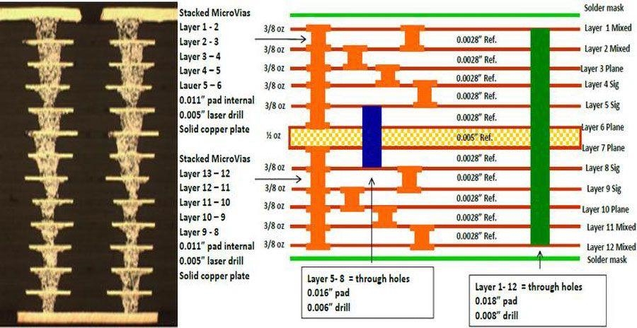
HDI PCB design operates on several core principles that distinguish it from standard PCB layouts. One key aspect is the use of microvias, which are tiny holes drilled into the board to connect layers. These vias are much smaller than traditional through hole vias, allowing for denser routing. According to industry standards like IPC-2226, microvias must meet specific aspect ratio and reliability criteria to ensure performance.
Another principle is the implementation of finer trace widths and spacing. HDI boards often feature lines as narrow as 3 mils or less, demanding precision in design and manufacturing. This enables more circuits in a limited area but requires careful attention to signal integrity. Layer stacking is also critical, with HDI designs often using build up technology to add layers sequentially, enhancing density.
For hobbyists, grasping these principles means recognizing the need for tighter tolerances and advanced techniques. Signal crosstalk and impedance control become more significant in HDI layouts due to the proximity of traces. Familiarity with standards such as IPC-6012E, which governs rigid board performance, helps ensure that designs meet reliability expectations.
Key Challenges for HDI Beginners
Starting with HDI PCB design as a beginner comes with unique challenges. The precision required for fine traces and microvias often exceeds the capabilities of basic design tools or manufacturing processes available to hobbyists. This can lead to issues like trace breakage or via failure if not addressed properly.
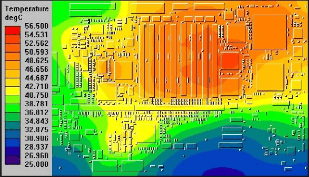
Thermal management is another concern. With components packed closely, heat dissipation becomes harder to manage. Without proper planning, hotspots can degrade performance or damage the board. Additionally, signal integrity issues, such as interference between closely spaced traces, require careful routing strategies to avoid problems.
Cost is a practical hurdle for many HDI beginners. The advanced materials and processes involved in HDI manufacturing often result in higher expenses compared to standard PCBs. However, by focusing on simpler HDI configurations initially, hobbyists can mitigate some of these challenges while building expertise.
Related Reading: HDI PCB Design: Overcoming Challenges in High-Density Interconnect
Practical Tips for Starting an HDI Project Easy
Embarking on an HDI project easy begins with a solid foundation in design practices tailored for beginners. First, start with a simple design that incorporates basic HDI features, such as a two layer build up with microvias. This reduces complexity while allowing you to learn key concepts. Focus on a small scale project, like a sensor module, to test your skills.
Next, pay attention to layer stack planning. Define the number of layers and their purpose early in the design phase. For instance, dedicate specific layers for power and ground planes to minimize noise. Adhering to guidelines from IPC-2226 for HDI stack up design ensures that your configuration supports signal integrity.
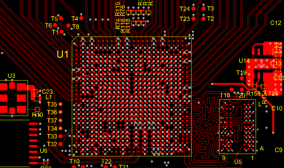
Routing is another critical area. Keep traces as short as possible to reduce signal delays, and avoid sharp bends that can cause reflections. Use rounded corners for traces whenever feasible. For microvias, ensure they are placed strategically to connect layers without overcrowding, following aspect ratio limits outlined in relevant standards.
Finally, simulate your design before manufacturing. Many design tools offer simulation features to check for signal integrity and thermal issues. This step can save time and resources by identifying potential flaws early. As an HDI beginner, these practices provide a manageable entry point into complex designs.
Best Practices for HDI PCB Design
To excel in HDI PCB design, hobbyists should adopt best practices aligned with industry standards. Begin by selecting appropriate materials that support fine line etching and microvia reliability. Materials with low dielectric constants can help manage signal speeds effectively, as per recommendations in IPC-4101 for laminate specifications.
Related Reading: Advanced HDI PCB Stackup Materials for Improved Signal Performance
When designing, maintain consistent trace widths and spacing to avoid manufacturing defects. Standards like IPC-6012E emphasize the importance of uniformity in trace geometry for performance. Additionally, incorporate adequate clearance between traces to prevent crosstalk, especially in high density areas.
Via placement requires careful thought. Use staggered or stacked microvias to optimize space, but ensure they meet reliability criteria set by IPC-2226. Avoid placing vias directly under components unless necessary, as this can complicate assembly and rework.
Testing is vital for any HDI project. After design completion, conduct thorough checks for continuity and shorts. If possible, perform a design rule check based on manufacturing capabilities to catch errors. These practices, grounded in established guidelines, help ensure a successful HDI PCB guide how to for beginners.
Resources for Learning HDI PCB Design
For hobbyists eager to dive into HDI PCB design, several non commercial resources provide valuable knowledge. Industry standards such as IPC-A-600K offer detailed insights into acceptable board conditions, including HDI specific criteria. This document is a must read for understanding quality expectations.
Technical publications from organizations like IPC also cover HDI design fundamentals. These resources often include guidelines on microvia technology and stack up strategies, making them ideal for an HDI beginner. Academic papers on PCB miniaturization can further enhance understanding of theoretical aspects behind HDI.
Online forums and communities focused on electronics design often share practical tips and tutorials. While engaging with these platforms, focus on discussions around standards and best practices rather than specific tools or brands. Building a library of such resources equips you with the knowledge needed for an HDI project easy.
Conclusion
HDI PCB design represents a significant leap for electronic hobbyists looking to create compact and efficient circuits. By understanding its principles, addressing common challenges, and following practical tips, beginners can confidently approach their first HDI project easy. This guide has outlined the essentials, from microvia usage to layer stacking, ensuring that you have a clear HDI PCB guide how to. Embracing best practices and leveraging industry standards like IPC-6012E and IPC-2226 ensures reliability in your designs. As an HDI beginner, starting small and building skills over time will lead to mastery of this advanced technology. Dive into the resources available, apply the knowledge shared, and elevate your electronics projects to new heights.
FAQs
Q1: What is the simplest way to start an HDI project easy as a beginner?
A1: For an HDI beginner, begin with a small scale design using minimal layers, such as a two layer HDI build up. Focus on basic features like microvias for layer connections. Use free or accessible design tools to practice layout and routing. Stick to simple projects like LED modules to learn without overwhelming complexity, ensuring a smooth entry into HDI technology.
Q2: How can I access a reliable HDI PCB guide how to for learning?
A2: Look for resources based on industry standards like IPC-2226, which covers HDI design principles. Technical publications from non commercial organizations provide detailed explanations on stack ups and microvias. Online communities focused on electronics often share beginner friendly tips. Building knowledge from these sources creates a solid foundation for HDI PCB design.
Q3: What challenges should an HDI beginner expect in their first project?
A3: As an HDI beginner, expect challenges like managing fine traces and microvias, which require precision. Signal integrity issues may arise due to dense layouts, and thermal management can be tricky in compact designs. Cost is also a factor, as HDI processes are pricier. Start with simple designs to minimize these hurdles while gaining experience.
Q4: Why is HDI PCB design important for hobbyist projects?
A4: HDI PCB design is vital for hobbyists aiming to create compact, high performance devices like wearables or IoT gadgets. It allows more components in less space, improving efficiency. For an HDI beginner, learning this technology means staying relevant with modern electronics trends. It also enhances skills in handling complex layouts for future projects.
References
IPC-6012E — Qualification and Performance Specification for Rigid Printed Boards. IPC, 2020.
IPC-2226 — Design Standard for High Density Interconnect (HDI) Printed Boards. IPC, 2003.
IPC-A-600K — Acceptability of Printed Boards. IPC, 2020.
IPC-4101 — Specification for Base Materials for Rigid and Multilayer Printed Boards. IPC, 2021.


