Introduction
Heavy copper PCBs play a vital role in modern electronics, particularly for applications requiring high current handling and superior thermal management. These specialized circuit boards feature copper layers significantly thicker than standard designs, often exceeding 3 ounces per square foot. For electrical engineers, understanding the benefits and applications of heavy copper PCBs is essential when designing systems that must manage heat dissipation effectively and ensure reliability under demanding conditions. This article explores the technical foundations, advantages, and practical uses of heavy copper PCBs, providing actionable insights for professionals tackling high-power challenges in industries like automotive, industrial controls, and power electronics.
What Is Heavy Copper PCB and Why It Matters
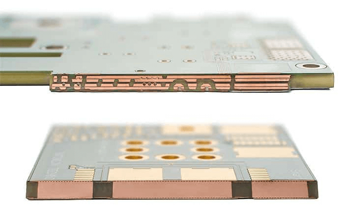
Heavy copper PCBs are defined by their increased copper thickness, typically ranging from 3 to 20 ounces per square foot or more, compared to the standard 1 or 2 ounces found in conventional boards. This enhanced copper weight allows them to carry higher currents and dissipate heat more efficiently, addressing critical needs in high-power applications. For electrical engineers, these boards are indispensable in scenarios where thermal stress and current density could compromise performance or safety.
The importance of heavy copper PCBs lies in their ability to support robust power distribution while maintaining structural integrity. They reduce the risk of thermal hotspots and electrical failures, extending the lifespan of electronic systems. Industries relying on consistent performance under extreme conditions, such as renewable energy and military electronics, often specify these boards to meet stringent reliability requirements.
Technical Principles of Heavy Copper PCBs
The core principle behind the heavy copper PCB is their capacity to handle elevated current loads and thermal energy. Copper, as a conductor, offers low electrical resistance, and increasing its thickness proportionally enhances current-carrying capability. According to widely recognized industry standards like IPC-2152, which governs current-carrying capacity, thicker copper traces require less width to manage the same current, optimizing board space.
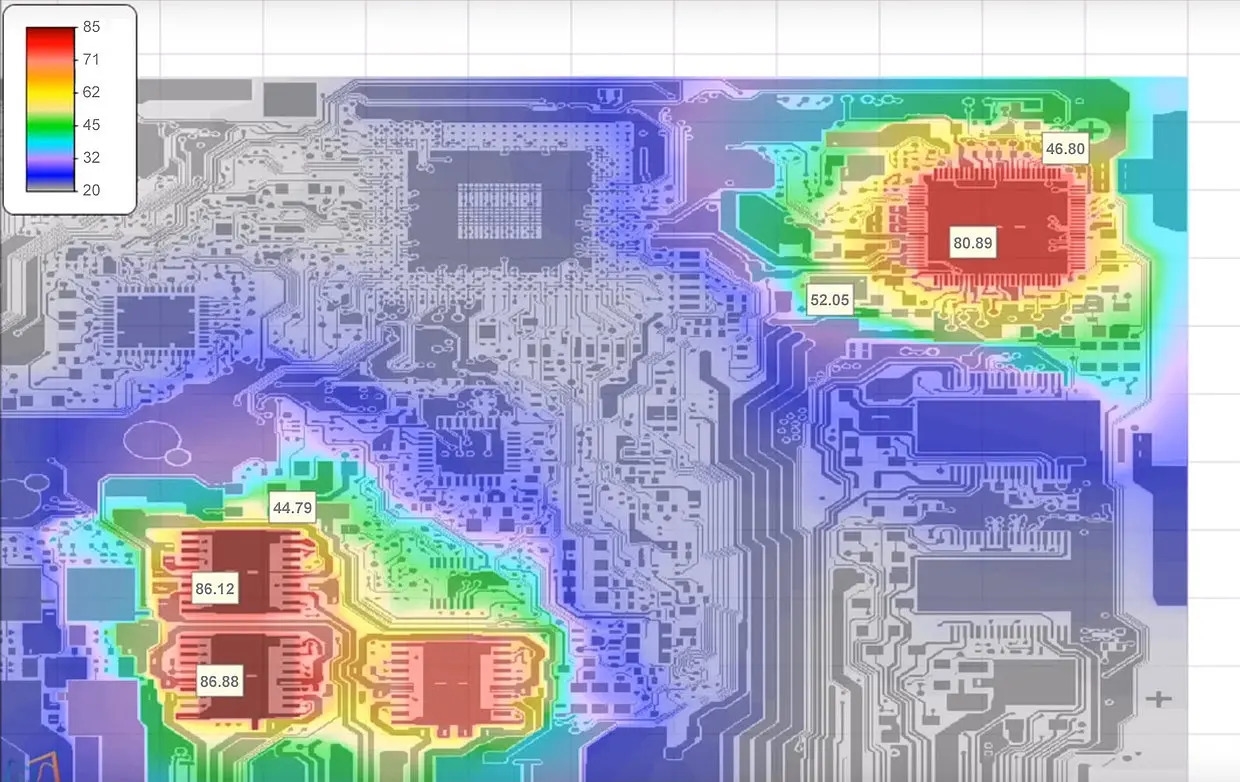
Thermal dissipation is another key mechanism. Thicker copper acts as a heat spreader, distributing thermal energy across the board and away from critical components. This reduces localized heating, a common cause of component failure. The thermal conductivity of copper, combined with strategic layer stacking, ensures efficient heat transfer to external sinks or ambient environments, maintaining operational stability.
Manufacturing heavy copper PCBs involves specialized processes to ensure uniform copper deposition and adhesion. Etching thicker copper requires precise control to avoid undercutting or trace damage, aligning with standards such as IPC-6012E for rigid printed board performance. These technical aspects underscore why heavy copper designs are tailored for high-stress applications.
Benefits of Heavy Copper PCBs for Electrical Engineers
Heavy copper PCBs offer several advantages that directly address engineering challenges in high-power systems. Below are the primary benefits with detailed explanations.
Enhanced Current Carrying Capacity
With thicker copper traces, these PCBs can handle significantly higher currents without overheating or degrading. This is crucial for power electronics where large currents are common. By reducing trace width needs, as guided by IPC-2152, engineers can design more compact layouts without sacrificing performance.
Superior Heat Dissipation Management
Managing heat dissipation is a critical concern in modern electronics. Heavy copper PCBs excel in spreading and dissipating thermal energy, preventing hotspots that could damage components. This property is vital in applications like motor drives or power supplies, where sustained heat generation occurs.
Increased Mechanical Strength
The added copper thickness improves the board's durability, making it resistant to mechanical stress and vibration. This is particularly beneficial in harsh environments, such as automotive or industrial settings, where boards must endure physical strain without cracking or delaminating.
Improved Reliability and Longevity
By mitigating thermal and electrical stress, heavy copper PCBs enhance system reliability. They reduce failure rates in high-power circuits, aligning with quality expectations outlined in IPC-A-600K for printed board acceptability. This reliability translates to lower maintenance costs and extended product life.
Applications of Heavy Copper PCBs in Industry
Heavy copper PCBs find extensive use across various sectors due to their unique properties. Electrical engineers often specify these boards for the following applications.
Power Electronics and Converters
In power supplies, inverters, and converters, heavy copper PCBs manage high currents and heat dissipation effectively. They ensure stable operation under continuous load, supporting efficient energy conversion in industrial and renewable energy systems.
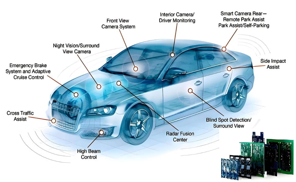
Automotive Electronics
Modern vehicles rely on complex electronics for engine control, battery management, and electric drivetrains. This type of automotive electronics PCB provides the necessary current capacity and thermal management for these systems, enduring the vibration and temperature extremes of automotive environments.
Industrial Control Systems
Industrial automation equipment, such as motor controllers and programmable logic controllers, often operates under high power and thermal stress. Heavy copper PCBs support robust performance, ensuring uptime and safety in manufacturing environments.
Military and Aerospace Systems
In military and aerospace applications, reliability is non-negotiable. Heavy copper PCBs meet stringent requirements for power distribution and heat management, performing consistently in extreme conditions like high altitude or combat scenarios.
Best Practices for Designing with Heavy Copper PCBs
For electrical engineers, designing with heavy copper PCBs requires careful consideration of several factors to maximize their benefits. Below are practical guidelines aligned with industry standards.
Optimize Trace Width and Spacing
Use design tools to calculate trace widths based on current requirements, referencing IPC-2152 for accurate sizing. Ensure adequate spacing to prevent short circuits, especially with thicker copper that may require adjusted etching processes.
Incorporate Thermal Vias and Heat Sinks
Integrate thermal vias to transfer heat from inner layers to external surfaces. Pairing heavy copper PCBs with external heat sinks enhances dissipation, maintaining component temperatures within safe limits.
Balance Copper Distribution
Uneven copper distribution can lead to warping during manufacturing or operation. Distribute copper symmetrically across layers to minimize stress, adhering to guidelines in IPC-6012E for performance specifications.
Test for Thermal Performance
Simulate thermal behavior during the design phase using appropriate software. Validate designs through physical testing to confirm heat dissipation capabilities, ensuring alignment with expected operational conditions.
Challenges and Considerations
While heavy copper PCBs offer significant advantages, they present certain challenges. Manufacturing complexity increases with thicker copper, potentially raising costs due to specialized etching and plating processes. Additionally, the added weight may impact applications where lightweight designs are critical. Engineers must weigh these factors against performance needs, ensuring the design justifies the investment.
Compatibility with standard assembly processes is another consideration. Thicker copper may require adjusted soldering parameters to avoid thermal damage, aligning with soldering standards like JEDEC J-STD-020E for component sensitivity. Careful planning during the design and manufacturing stages mitigates these issues, ensuring successful implementation.
Conclusion
Heavy copper PCBs stand out as a powerful solution for electrical engineers addressing high current and thermal management challenges. Their benefits, including enhanced current capacity, superior heat dissipation, and increased reliability, make them indispensable in demanding applications across automotive, industrial, military, and power electronics sectors. By understanding their technical principles and adhering to best practices, engineers can leverage these boards to design robust, efficient systems. Following industry standards ensures optimal performance, making heavy copper PCBs a cornerstone of modern high-power electronics design.
FAQs
Q1: What defines a heavy copper PCB and its primary benefit?
A1: A heavy copper PCB features copper layers thicker than 3 ounces per square foot, distinguishing it from standard boards. Its primary benefit is the ability to handle high currents and manage heat dissipation effectively. This makes it ideal for power electronics, ensuring reliability under thermal stress by distributing heat evenly and preventing component failure in demanding environments.
Q2: How do heavy copper PCBs manage heat dissipation in high-power systems?
A2: Heavy copper PCBs manage heat dissipation by utilizing thicker copper layers to spread thermal energy across the board. This reduces hotspots and transfers heat away from critical components. When paired with thermal vias or heat sinks, they maintain stable temperatures, protecting system integrity in high-power applications like inverters or motor controllers.
Q3: What are common applications of heavy copper PCBs for engineers?
A3: Heavy copper PCBs are widely used in power electronics, automotive systems, industrial controls, and military equipment. Their ability to support high currents and manage heat dissipation makes them suitable for applications requiring robust performance. Engineers rely on these boards for consistent operation in environments with extreme electrical and thermal demands.
Q4: Are there limitations to using heavy copper PCBs in design?
A4: Yes, heavy copper PCBs can present challenges like higher manufacturing costs due to specialized processes. Their added weight may not suit lightweight applications. Engineers must balance these limitations against benefits like enhanced heat dissipation and durability, ensuring the design aligns with project requirements and operational constraints.
References
IPC-2152 — Standard for Determining Current Carrying Capacity in Printed Board Design. IPC, 2009.
IPC-6012E — Qualification and Performance Specification for Rigid Printed Boards. IPC, 2020.
IPC-A-600K — Acceptability of Printed Boards. IPC, 2020.
JEDEC J-STD-020E — Moisture/Reflow Sensitivity Classification for Nonhermetic Surface Mount Devices. JEDEC, 2014.


