Introduction
Printed circuit boards form the backbone of modern electronics, carrying signals and power through intricate copper pathways. Engineers often face the choice between standard PCBs and heavy copper PCBs, each suited to different demands. Standard boards typically feature copper thicknesses of 1 ounce per square foot or less, handling everyday applications efficiently. Heavy copper PCBs, with thicknesses starting at 3 ounces and reaching up to 20 ounces or more, cater to high-power scenarios where reliability under stress is paramount. This comparison of heavy copper PCB vs standard PCB highlights key differences in performance, cost, and suitability. Understanding these aspects helps electrical engineers select the optimal board for their designs.
What Is a Heavy Copper PCB and Why Does It Matter?
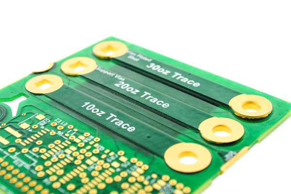
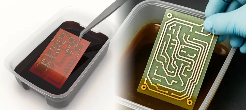
A standard PCB uses thin copper layers, usually 0.5 to 2 ounces per square foot, which equates to about 18 to 70 microns in thickness. These boards excel in high-density signal routing for consumer electronics and telecommunications. In contrast, a heavy copper PCB incorporates thicker copper foils, often 3 ounces or greater, enabling robust current handling and thermal management. The distinction arises during fabrication, where heavy copper requires specialized plating and etching processes to build up thickness uniformly.
This matters in industries pushing power limits, such as renewable energy systems and industrial controls. Standard PCBs may overheat or fail under sustained high currents, leading to reliability issues. Heavy copper boards mitigate these risks, supporting denser power delivery in compact spaces. For electrical engineers, choosing heavy copper aligns with application needs, ensuring compliance with performance expectations without unnecessary overdesign.
Key Technical Differences Between Heavy Copper and Standard PCBs
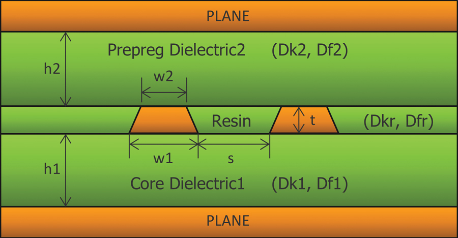
The primary difference lies in copper weight, which directly impacts electrical resistance and heat dissipation. Thicker copper in heavy boards reduces resistance per unit length, allowing higher current densities before reaching thermal limits. Standard PCBs prioritize fine-line etching for signal integrity, with trace widths often below 0.1 mm. Heavy copper demands wider traces to maintain manufacturability, as etching deeper into thick foil risks undercuts and nonuniformity.
Mechanically, heavy copper introduces greater stress during lamination and drilling due to thermal expansion mismatches. This can lead to warpage, addressed through controlled pressing cycles and symmetric stackups. Electrically, heavy copper excels in power planes, minimizing voltage drops over long traces. Signal propagation, however, may suffer from increased inductance in very thick layers, requiring careful impedance control.
Fabrication tolerances tighten for heavy copper, with plating buildup ensuring even thickness across panels. Standard processes suffice for thin foils, but heavy variants need sequential buildup to avoid defects like voids. These principles guide engineers in balancing power and signal requirements within board constraints.
Advantages and Disadvantages of Heavy Copper PCBs
Heavy copper PCBs offer superior current-carrying capacity, often handling several times more amperage than standard boards without excessive heating. This stems from lower resistance and better thermal conductivity, ideal for power converters and motor drives. Enhanced mechanical strength resists vibration and thermal cycling, extending service life in harsh environments. Additionally, fewer vias are needed for current distribution, simplifying routing and reducing assembly complexity.
Despite these benefits, heavy copper PCB advantages come with trade-offs. Manufacturing challenges include longer plating times and higher defect risks during etching, potentially increasing scrap rates. Boards may exhibit more warpage post-lamination, necessitating fixturing during assembly. For high-frequency signals, thicker copper can degrade performance through skin effect losses, limiting use in RF applications.
Cost escalates due to material volume and process complexity, making heavy copper less viable for low-power prototypes. Engineers must weigh these heavy copper PCB advantages disadvantages against project goals, opting for hybrids where power and signal zones coexist.
Heavy Copper PCB Cost Factors
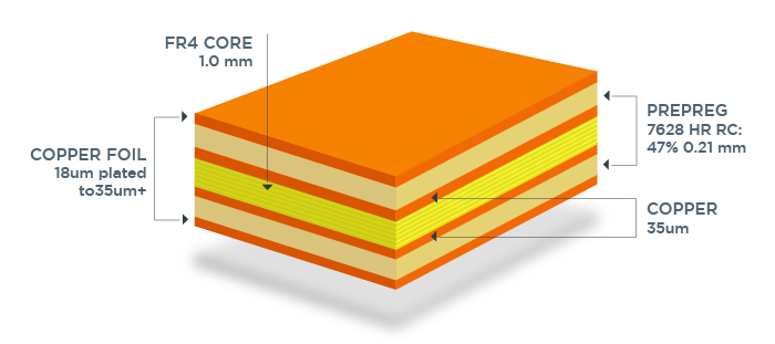
Material costs dominate, as heavy copper requires significantly more foil and plating chemistry per panel. Standard PCBs use readily available thin laminates, keeping expenses low for volume production. Heavy copper demands premium substrates with higher Tg to withstand plating baths, further inflating bills of materials. Etching solutions must handle deeper penetration, consuming more volume and generating additional waste treatment expenses.
Process overhead includes extended cycle times for buildup plating, often doubling or tripling standard runs. Yield suffers from issues like over-etching or plating voids, requiring tighter process controls and inspections. For prototypes, heavy copper PCB cost can exceed standard by 2-5 times, though economies scale in high-volume power applications. Engineers factor in lifecycle savings from reduced failures when justifying premiums.
Assembly adds nuance, with heavier boards needing reinforced soldering profiles to avoid tombstoning on thick pads. Tooling for routing and drilling wears faster, amortizing over larger panels. Procurement teams optimize by specifying minimum viable thickness, blending zones of heavy and standard copper where feasible.
Performance Comparison: Heavy Copper vs Standard PCB
In power delivery, heavy copper outperforms by distributing heat more evenly across traces and planes. Standard boards rely on thinner paths, prone to hotspots under load, which accelerate insulation degradation. Heavy variants maintain lower temperature rises, supporting higher power densities in constrained enclosures. Testing per industry guidelines reveals heavy copper's edge in thermal cycling endurance.
Signal integrity favors standard PCBs for their finer geometries and controlled impedances. Heavy copper's bulkier traces introduce parasitics, potentially causing crosstalk in mixed-signal designs. Mitigation involves segmented planes and stitching vias, but at added complexity. Overall, heavy copper PCB performance shines in DC-heavy or low-frequency power roles.
Reliability metrics, such as mean time between failures, improve with heavy copper in high-current scenarios. Standard boards suffice for battery-powered gadgets, where efficiency trumps raw capacity. Engineers simulate both via thermal and electrical models to predict behaviors accurately.
Manufacturing Best Practices for Heavy Copper PCBs
Start with stackup design emphasizing symmetry to minimize warpage, using core materials with matched CTE. Sequential lamination builds thickness incrementally, preventing delamination from copper shrinkage. Plating processes follow controlled current densities to ensure uniformity, with frequent thickness checks via coupons.
Etching employs tented vias and spray systems optimized for aspect ratios exceeding 1:1. Post-etch cleaning removes undercuts, preserving trace integrity. IPC-6012E outlines qualification for rigid boards, mandating electrical and mechanical tests post-fabrication. Bake-out precedes assembly to desorb moisture, critical for heavy copper's hygroscopic nature.
Assembly demands low standoff heights and nitrogen reflow to wet thick pads uniformly. IPC-A-600K defines acceptability criteria, guiding inspections for plating coverage and solderability. These practices ensure heavy copper boards meet performance without excessive rework.
Applications and Decision-Making Guidance
Heavy copper thrives in automotive inverters, where high currents demand robust dissipation. Industrial welders and UPS systems leverage its durability for continuous duty. Aerospace power modules benefit from vibration resistance, though weight constraints limit extremes. Standard PCBs dominate IoT sensors and processors, prioritizing density over power.
To choose, calculate required ampacity using trace width calculators based on rise temperatures. Assess space: heavy copper needs wider paths, potentially upsizing boards. Budget reviews total cost of ownership, including failures. Hybrid approaches layer heavy power planes under standard signal routing.
Consult fab capabilities early, verifying heavy copper experience. Simulate thermal profiles to validate choices. This systematic approach aligns heavy copper PCB vs standard PCB with engineering realities.
Conclusion
Selecting between heavy copper and standard PCBs hinges on power demands, thermal constraints, and economics. Heavy copper delivers unmatched current handling and reliability for demanding applications, despite higher costs and fabrication hurdles. Standard boards offer versatility and affordability for signal-focused designs. By evaluating heavy copper PCB advantages disadvantages, cost, and performance, engineers optimize outcomes. Reference standards like IPC-6012E and IPC-A-600K during design to ensure quality. The right board elevates product success.
FAQs
Q1: What is the main difference in heavy copper PCB vs standard PCB?
A1: Heavy copper PCBs feature copper thicknesses of 3 ounces per square foot or more, compared to 1-2 ounces in standard boards. This enables superior current capacity and heat management for power-intensive uses. Standard variants prioritize fine traces for signals. Factory insights emphasize sequential plating for uniformity in heavy copper, per IPC guidelines. Choose based on ampacity needs.
Q2: What are the heavy copper PCB advantages disadvantages?
A2: Advantages include higher thermal dissipation, mechanical strength, and fewer vias for power routing. Disadvantages involve elevated costs, warpage risks, and etching challenges. Performance suits high-current apps, but signals may need isolation. Balanced designs mitigate issues through symmetric stackups. Overall, benefits outweigh drawbacks in power electronics.
Q3: How does heavy copper PCB cost compare to standard?
A3: Heavy copper incurs higher material and process expenses due to thick foils and extended plating. Standard boards benefit from simpler, faster fabrication. Costs scale with volume, but prototypes see larger premiums. Factor in reliability gains for total ownership. Optimize by zoning heavy copper selectively.
Q4: What impacts heavy copper PCB performance?
A4: Thicker copper lowers resistance for better power delivery and heat spreading. It excels in low-frequency, high-current scenarios but may increase inductance for signals. Manufacturing per IPC-6012E ensures consistent metrics. Thermal simulations predict behaviors accurately. Performance aligns with application stresses.
References
IPC-6012E — Qualification and Performance Specification for Rigid Printed Boards. IPC, 2017
IPC-A-600K — Acceptability of Printed Boards. IPC, 2020
IPC-2221F — Generic Standard on Printed Board Design. IPC, 2020