Introduction
Magnetic Resonance Imaging (MRI) machines represent the pinnacle of medical diagnostic technology, relying on intricate electronic systems to generate high-resolution images. These systems process vast amounts of RF signals, manage gradient coils, and handle data acquisition under extreme electromagnetic conditions. High-density interconnect (HDI) PCBs play a critical role in enabling the compact, high-performance electronics required for modern MRI scanners. By incorporating microvias and finer trace geometries, HDI PCB for MRI applications allow engineers to pack more functionality into smaller spaces without compromising signal quality. This is essential in environments where space constraints and weight reduction directly impact machine design and patient comfort. However, integrating HDI technology into MRI systems introduces unique engineering hurdles that demand precise design and manufacturing control.
The demand for higher image resolution in MRI continues to drive the adoption of high-density MRI PCB designs. Engineers must balance miniaturization with unwavering reliability, as failures in these boards can disrupt critical scans. HDI structures address this by supporting advanced components like fine-pitch BGAs and high-speed interfaces. Yet, the challenges of thermal management and electromagnetic compatibility persist. This article explores the advantages, design rules, manufacturing processes, and obstacles of HDI PCBs in MRI machines.
What Are HDI PCBs and Why Do They Matter in MRI Machines?
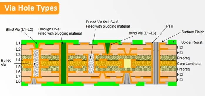
HDI PCBs differ from standard multilayer boards through their use of microvias, typically smaller than 150 micrometers in diameter, along with blind, buried, and stacked vias. These features enable higher routing density, finer line widths and spaces often down to 50 micrometers or less, and sequential build-up layers. Microvias in MRI PCBs are laser-drilled for precision, allowing connections between adjacent layers without penetrating the entire stackup. In MRI applications, such boards support the dense integration of ASICs, FPGAs, and RF amplifiers needed for real-time signal processing.
MRI machines require PCBs that handle high-frequency signals from RF coils while minimizing noise in strong magnetic fields. Traditional through-hole vias create stubs that degrade signal integrity, but HDI eliminates these through shorter interconnect paths. This results in reduced crosstalk and electromagnetic interference, vital for maintaining image fidelity. High-density MRI PCB designs also facilitate the miniaturization of receiver coils and gradient control modules, improving scanner accessibility for patients.
The relevance of HDI technology stems from the escalating complexity of MRI electronics. As field strengths increase to 3T or 7T, signal bandwidths widen, demanding boards with superior electrical performance. HDI PCBs meet these needs by supporting more I/O per component and better power distribution. Without them, MRI systems would require larger, heavier boards, complicating installation and cooling.
Advantages of HDI PCBs in MRI Applications
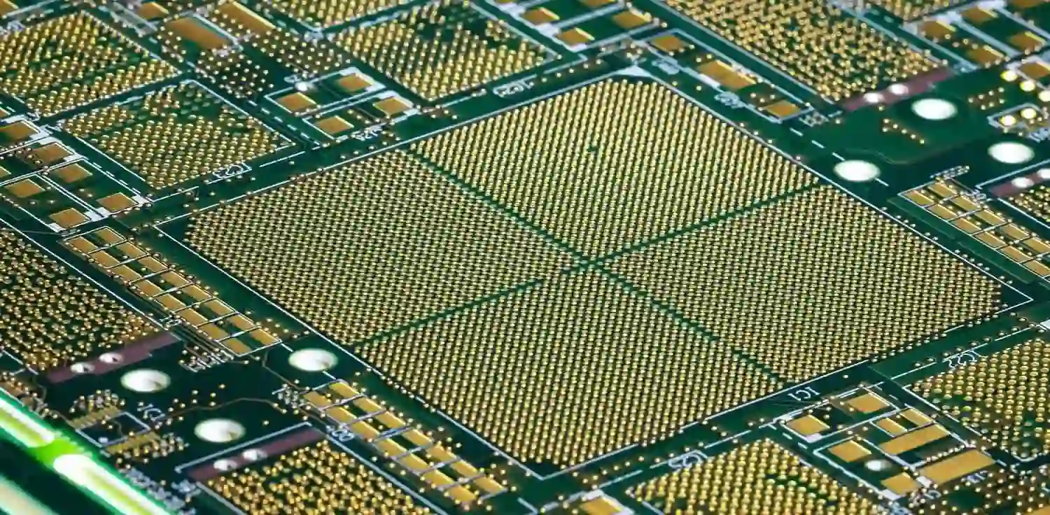
One primary advantage of HDI PCB for MRI is the dramatic increase in component density. Engineers can mount thousands of connections in a compact footprint, ideal for space-limited modules like digital receiver chains. This density supports the integration of high-pin-count devices essential for parallel data processing in MRI reconstruction.
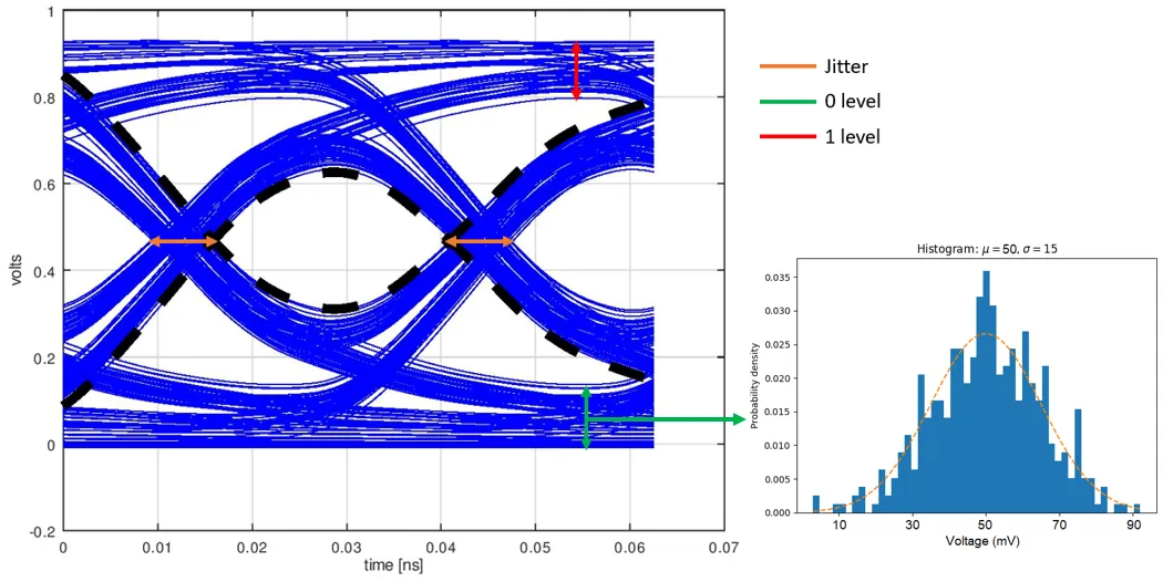
Superior signal integrity stands out as another key benefit. Shorter signal paths from microvias reduce attenuation, reflections, and timing skew, crucial for the gigahertz-range RF signals in MRI. This minimizes phase errors in k-space sampling, enhancing image quality. Additionally, lower inductance in HDI vias improves impedance control, aiding compliance with stringent EMI requirements in shielded scanner rooms.
HDI boards contribute to overall system reliability through reduced mechanical stress. Blind and buried vias distribute loads more evenly across layers, mitigating warpage during thermal cycling. In MRI environments, where boards endure repeated power surges from gradient pulses, this durability prevents microcracks. Weight savings from thinner stackups also ease handling during maintenance.
Thermal performance sees mixed gains with HDI PCB for MRI. While higher density can concentrate heat, embedded vias enable efficient heat spreading to planes. This supports higher power densities in amplifiers without excessive hotspots. Overall, these advantages enable sleeker MRI designs with faster scan times.
Challenges in Implementing HDI PCBs for MRI Machines
Despite the benefits, HDI PCB manufacturing introduces significant hurdles, starting with elevated costs due to sequential processes and specialized equipment. Laser drilling, via filling, and multiple plating cycles drive up expenses, particularly for low-volume MRI prototypes. Yield rates suffer from defects like via barrel cracks if processes deviate slightly.
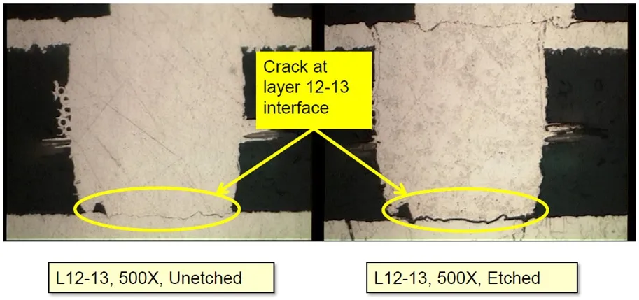
Reliability under MRI operating conditions poses another challenge. Microvias are susceptible to electromigration and CAF failures in high-current paths for gradient drivers. Thermal expansion mismatches between copper and dielectrics exacerbate this during rapid heating from RF pulses. Stacked microvias amplify stress concentrations, risking opens after thousands of cycles.
Design complexity demands adherence to strict HDI PCB design rules. Aspect ratios for microvias typically limit to 1:1 or less to ensure plating uniformity. In MRI, where boards must resist magnetic-induced eddy currents, non-magnetic fills and low-loss materials add constraints. Inspection via X-ray or cross-sectioning verifies integrity but slows development.
Electromagnetic challenges in MRI environments further complicate HDI integration. High-density traces can act as antennas for RF interference, requiring careful grounding and shielding strategies. Balancing density with isolation gaps tests engineer limits.
HDI PCB Design Rules and Best Practices for MRI Systems
Effective HDI PCB design for MRI begins with stackup planning per IPC-2226 guidelines. Microvia capture pads should exceed 150 micrometers, with annular rings at least 75 micrometers to prevent drill breakout. Line widths and spaces scale with class, often 40/40 micrometers for high-end boards. Aspect ratios stay below 0.8:1 for reliable plating.
For microvias in MRI PCBs, prefer staggered configurations over stacked to distribute thermomechanical stress. This enhances reliability in via chains subjected to MRI's pulsed operations. Via-in-pad designs optimize density but require planarization to avoid solder voids.
Material selection focuses on low Dk/Df laminates for RF integrity. Controlled impedance traces, verified via TDR, ensure signal fidelity. Power integrity demands decoupled planes with microvia stitching.
Best practices include design rule checks for via fanout and escape routing under BGAs. Simulate SI/PI early to preempt issues. Prototype iterations refine rules for specific MRI frequencies.
HDI PCB Manufacturing Processes for High-Density MRI PCBs
HDI PCB manufacturing for MRI follows a sequential build-up flow. Core layers receive UV laser drilling for microvias, followed by desmear and sequential lamination. Copper electroplating fills vias, with planarization via etch-back or molding compounds. Multiple iterations build outer layers.
IPC-6016 qualification ensures performance through thermal shock, vibration, and electrical tests tailored to medical rigor. Plasma cleaning enhances adhesion, while automated optical inspection detects voids. Final boards undergo flying probe for continuity.
For MRI, non-conductive via fills prevent shorts in magnetic fields. Bake-out controls moisture per J-STD-020 to avoid popcorn effects during reflow.
Conclusion
HDI PCBs revolutionize MRI machines by delivering compactness, signal excellence, and density unattainable with conventional boards. While advantages in performance and size prevail, challenges in design, reliability, and cost require disciplined engineering. Adhering to proven rules and processes unlocks their potential. As MRI evolves, HDI will remain central to advancing diagnostic precision.
FAQs
Q1: What are the main advantages of HDI PCB for MRI machines?
A1: HDI PCB for MRI provides higher component density for compact modules, superior signal integrity via shorter microvia paths, and reduced EMI for clean RF processing. These enable faster scans and higher resolution without enlarging systems. Reliability improves through even stress distribution, critical for pulsed operations. Overall, they support advanced imaging in space-constrained designs.
Q2: How do microvias in MRI PCBs enhance performance?
A2: Microvias in MRI PCBs, under 150 micrometers, eliminate via stubs for better high-frequency response and lower crosstalk. They allow dense routing for data-heavy boards, improving image reconstruction speed. Staggered placements boost thermal cycling endurance. This directly aids precise k-space filling in high-field scanners.
Q3: What are essential HDI PCB design rules for MRI applications?
A3: Key HDI PCB design rules include microvia diameters below 150 micrometers, aspect ratios under 1:1, and minimum line/space of 50 micrometers. Per IPC-2226, ensure adequate annular rings and impedance control. For MRI, prioritize low-loss materials and SI simulations to handle RF demands.
Q4: What challenges arise in HDI PCB manufacturing for high-density MRI PCBs?
A4: HDI PCB manufacturing challenges include low yields from via plating defects, high costs for sequential builds, and reliability risks like electromigration. MRI specifics demand magnetic-compatible fills and rigorous IPC-6016 testing. Thermal management intensifies with density, requiring advanced cooling integration.
References
IPC-2226 - Sectional Design Standard for High Density Interconnects. IPC
IPC-6016D - Qualification and Performance Specification for High Density Interconnect (HDI) Printed Boards. IPC
J-STD-020E - Moisture/Reflow Sensitivity Classification for Nonhermetic Surface Mount Devices. JEDEC