Introduction
In the realm of printed circuit board (PCB) maintenance, moving beyond basic soldering and visual inspections requires mastery of sophisticated methods tailored for modern electronics. Component-level PCB repair training equips electric engineers with the precision needed to address failures in densely packed assemblies, where surface-mount devices (SMDs), ball grid arrays (BGAs), and fine-pitch components dominate. These advanced techniques not only salvage high-value boards but also minimize downtime in critical applications like telecommunications and medical devices. As PCB densities increase, engineers must adopt advanced SMD rework techniques, micro soldering for PCB repair, the BGA reballing process, and systematic troubleshooting for complex PCB failures. This article explores these methods in depth, providing practical guidance grounded in engineering principles. By understanding these skills, professionals can enhance reliability and extend the lifecycle of electronic systems.
Understanding Component-Level PCB Repair
Component-level PCB repair involves diagnosing and replacing individual components on a board while preserving the integrity of surrounding circuitry and the substrate itself. Unlike board-level fixes, this approach demands high-resolution tools and controlled processes to handle pitches below 0.5 mm and multilayer stacks. Electric engineers pursuing component level PCB repair training learn to isolate faults using electrical testing, thermal imaging, and continuity checks before physical intervention. The relevance stems from the escalating complexity of consumer and industrial electronics, where a single failed IC can render an entire assembly obsolete. Mastering these skills reduces scrap rates and supports sustainability efforts in electronics manufacturing. Ultimately, it empowers engineers to tackle repairs that were once considered uneconomical.
This repair paradigm matters because modern PCBs integrate heterogeneous components, from passives to high-I/O BGAs, exposed to thermal cycling, vibration, and environmental stressors. Failures often manifest as intermittent signals or parametric drifts, necessitating advanced diagnostics over simple continuity probes. Training programs emphasize hands-on practice with rework stations to build muscle memory for precision tasks. Engineers benefit from structured curricula that cover thermal profiles, stencil alignment, and post-repair verification. In high-reliability sectors, such expertise aligns with quality benchmarks like those in IPC-7711B/7721B for rework procedures.
Advanced SMD Rework Techniques
Advanced SMD rework techniques extend beyond drag soldering to include precise hot air reflow, infrared heating, and vacuum-assisted removal for components like QFNs and LQFP packages. Engineers begin by profiling the thermal cycle to match the component's JEDEC moisture sensitivity level, preventing delamination during heating. A key step involves applying low-residue flux and using a focused nozzle to desolder pads without lifting traces or damaging vias. Preheating the board to 100-150°C stabilizes the assembly, reducing thermal shock across copper layers. Post-removal, site dressing with fiberglass abrasives prepares pads for new device placement, ensuring flatness for reliable solder joints.
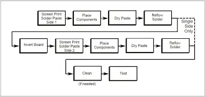
Alignment under a stereo microscope at 10-40x magnification guarantees coplanarity, followed by controlled reflow with thermocouples monitoring peak temperatures around 220-260°C. Advanced practitioners employ split-beam optics for shadow-free viewing and integrate X-ray for hidden joint inspection. These techniques demand practice to avoid common pitfalls like tombstoning, caused by uneven heating gradients. Component level PCB repair training often simulates real-world scenarios with daisy-chained test boards to hone these skills. By adhering to thermal guidelines in J-STD-001G, engineers achieve void-free joints that withstand accelerated life testing.
Related Reading: The Ultimate Guide to Choosing the Right Manual Soldering Station for SMD Rework
Micro Soldering for PCB Repair
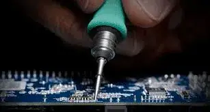
Micro soldering for PCB repair targets ultra-fine pitches down to 0.2 mm, using specialized irons with 0.1-0.3 mm tips and temperature-controlled stations set to 300-350°C. This method excels for repairing BGAs, connectors, and discretes on flex or rigid-flex boards, where access is obstructed by shielding or dense routing. Engineers apply thin flux layers and hand-form leads with tweezers before tacking corners for stability. Drag soldering with 0.3 mm wire follows, minimizing bridges through wick and isopropyl alcohol cleaning. Thermal management prevents pad erosion by limiting dwell time to 2-3 seconds per joint.
Challenges arise from oxidation on aged pads, addressed by activation fluxes and nitrogen purging to inhibit IMC growth. Post-solder, electrical testing verifies continuity and insulation resistance above 100 MΩ. Training emphasizes ergonomic positioning and anti-static protocols to safeguard ESD-sensitive devices. Micro soldering integrates with flying probe testers for in-circuit validation, ensuring functionality before reassembly. These practices align with IPC-A-610H criteria for class 3 assemblies, where joint fillet heights must exceed 75% of lead thickness.
The BGA Reballing Process
The BGA reballing process restores failed or migrated solder spheres on high-density packages, critical for servers and automotive modules with 1000+ I/Os. Engineers start with stencil printing of solder paste spheres, typically 0.3-0.76 mm diameter, matched to original alloy like SAC305. Reflow in a convection oven profiles to 245-260°C peak, with linear ramps to control wetting. X-ray pre-inspection identifies missing or bridged balls, guiding selective reballing. Post-process, shear testing confirms adhesion strength above 1500 gf per ball.
Site preparation involves interposer removal via hot air at 350°C, followed by flux dipping and reflow onto the PCB. Advanced setups use laser-assisted alignment for sub-10 μm accuracy. Common issues like head-in-pillow defects stem from paste volume mismatches, mitigated by volume metering. Component level PCB repair training includes mock BGA stations to practice cycle times under 30 minutes. This process adheres to IPC-7711B/7721B guidelines for ball attach integrity.
Troubleshooting Complex PCB Failures
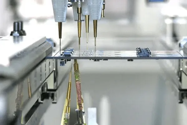
Troubleshooting complex PCB failures requires a layered approach: functional, boundary scan, and thermal analysis to pinpoint root causes like latent opens or cracked die. Electric engineers initiate with schematic review and signal integrity simulation to hypothesize failure modes. In-circuit emulation probes dynamic behaviors, while curve tracers reveal parametric shifts in passives. For multilayer boards, time-domain reflectometry detects impedance discontinuities from via stubs.
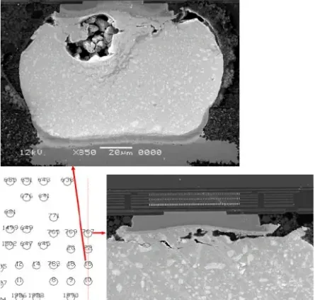
Advanced diagnostics employ lock-in thermography to visualize heat signatures from leaky junctions, isolating faults non-destructively. Acoustic microscopy reveals subsurface delams, guiding decap for die inspection. Data logging during environmental stress correlates failures to thermal expansion mismatches. Practical workflows prioritize non-invasive tests before component removal.
Boundary scan chains, per IEEE 1149.1, automate netlist verification, flagging stuck-at faults. Engineers document findings in failure analysis reports, iterating root cause via fishbone diagrams. Training simulates no-fault-found scenarios to build deductive skills. These methods reduce mean time to repair below 4 hours for field returns.
Best Practices in Advanced PCB Repair
Integrating these techniques demands a cleanroom environment with ESD flooring and ionized air to below 100 V/cm. Engineers calibrate tools daily, verifying hot air profiles against master thermocouples. Documentation tracks process parameters, enabling traceability for audits. Cross-training in multiple methods fosters versatility across assembly types.
Preventive measures like conformal coating inspection precede repairs, stripping only as needed with plasma cleaners. Post-repair bake-out at 125°C for 24 hours drives off moisture before functional test. Collaboration with design teams refines DFM rules, reducing future repair needs.
Related Reading: Troubleshooting PCB Tools: A Practical Guide for Diagnosing and Repairing Boards
Conclusion
Advanced techniques in component-level PCB repair empower electric engineers to conquer the challenges of modern electronics. From advanced SMD rework techniques and micro soldering for PCB repair to the BGA reballing process and troubleshooting complex PCB failures, these skills demand precision and methodical execution. Component level PCB repair training bridges theory and practice, aligning with standards like IPC-7711B/7721B, J-STD-001G, and IPC-A-610H. By adopting these methods, professionals enhance board yields, cut costs, and uphold reliability in demanding applications. Continuous practice and tool proficiency remain key to excellence in this evolving field.
FAQs
Q1: What does component level PCB repair training typically cover for electric engineers?
A1: Component level PCB repair training focuses on hands-on skills like advanced SMD rework techniques, micro soldering for PCB repair, and BGA reballing. Engineers learn thermal profiling, X-ray inspection, and post-repair validation to handle fine-pitch assemblies. Practical sessions use test boards to simulate real failures, emphasizing safety and ESD control. This builds confidence for high-reliability repairs without board replacement.
Q2: How do advanced SMD rework techniques differ from basic methods?
A2: Advanced SMD rework techniques employ hot air stations with split nozzles and precise thermocouples, unlike basic irons. They match reflow profiles to component specs per J-STD-001G, preventing warpage. Vacuum pick-up and stencil site dressing ensure clean pad preparation. These yield class 3 joints, verified by dye-and-peel testing for voids under 25%.
Q3: What are the critical steps in the BGA reballing process?
A3: The BGA reballing process includes package removal, site cleaning, stencil printing of solder spheres, reflow, and X-ray inspection. Flux selection prevents oxidation, with profiles peaking at 260°C. Alignment tolerances stay below 50 μm. Engineers verify ball shear strength post-process, aligning with IPC-7711B/7721B for attach quality.
Q4: How can engineers effectively troubleshoot complex PCB failures?
A4: Troubleshooting complex PCB failures starts with thermal imaging and boundary scan to isolate issues non-invasively. Schematic correlation and TDR pinpoint opens or crosstalk. Decap follows for die analysis if needed. Logging under stress reveals intermittent modes, reducing diagnosis time through systematic layering.
References
IPC-7711B/7721B — Rework, Modification and Repair of Electronic Assemblies. IPC, 2018
J-STD-001G — Requirements for Soldered Electrical and Electronic Assemblies. IPC, 2011
IPC-A-610H — Acceptability of Electronic Assemblies. IPC, 2019