Introduction
High-frequency PCB design is a critical aspect of modern electronics, where signal integrity directly impacts performance. As devices operate at gigahertz frequencies, challenges like signal loss and interference become prominent. Effective PCB routing techniques are essential to maintain data accuracy and system reliability in applications such as telecommunications, automotive radar, and IoT devices. This article explores proven strategies for minimizing signal degradation and crosstalk through optimized trace length, trace spacing, vias usage, and ground plane design. By adhering to industry standards and engineering principles, designers can achieve robust high-frequency performance. The focus remains on practical solutions for electrical engineers seeking to enhance their PCB layouts for demanding environments. Let us dive into the core concepts and best practices that ensure minimal signal loss and interference.
What Is High-Frequency PCB Routing and Why It Matters
High-frequency PCB routing refers to the process of designing trace paths on a printed circuit board to handle signals with frequencies typically above 100 MHz. At these frequencies, signals behave more like waves, making them susceptible to reflection, crosstalk, and attenuation. Poor routing can lead to significant signal loss, where energy dissipates as heat or noise, and interference, where adjacent signals disrupt each other. This impacts system performance, causing data errors or complete failure in critical applications like 5G networks or medical equipment. Proper routing ensures impedance matching, reduces electromagnetic interference (EMI), and maintains signal integrity. For engineers, mastering these techniques is not just about meeting specifications but also about ensuring reliability under real-world conditions. The stakes are high, and attention to detail in routing directly correlates with project success.
Technical Principles of Signal Loss and Interference in High-Frequency PCBs
Understanding the root causes of signal loss and interference is fundamental to effective PCB routing. Signal loss primarily occurs due to dielectric absorption, conductor resistance, and skin effect at high frequencies. Dielectric materials absorb signal energy, while conductor resistance increases as current flows near the surface of traces. Interference, on the other hand, arises from crosstalk between adjacent traces and external EMI sources. Both phenomena are exacerbated by improper trace geometry, mismatched impedances, and inadequate grounding.
Trace length plays a pivotal role in signal integrity. Longer traces increase propagation delay and risk signal reflection if not impedance-matched. Trace spacing affects crosstalk, as closely spaced traces couple electromagnetically, inducing unwanted noise. Vias, while necessary for multilayer designs, introduce discontinuities that can reflect signals or create parasitic inductance. Ground planes are crucial for providing a low-impedance return path, but poorly designed planes can lead to ground loops or uneven current distribution. These principles highlight the need for meticulous design to counteract inherent challenges in high-frequency environments.
Best Practices for High-Frequency PCB Routing
To mitigate signal loss and interference, engineers must adopt precise routing strategies grounded in established standards like those from IPC. Below are actionable techniques focusing on trace length, trace spacing, vias, and ground plane design.
Optimizing Trace Length for Signal Integrity
Trace length should be minimized to reduce propagation delays and signal attenuation. When longer traces are unavoidable, ensure controlled impedance by matching the trace dimensions to the characteristic impedance of the system, often 50 ohms for high-frequency designs. Avoid abrupt changes in trace direction to prevent reflections. Gradual bends with a radius of at least three times the trace width are recommended. Adhering to guidelines in IPC-2221B, which covers generic standard on printed board design, helps in calculating appropriate trace lengths for specific frequencies.
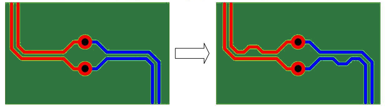
Maintaining Proper Trace Spacing to Reduce Crosstalk
Trace spacing is critical to minimizing electromagnetic coupling between adjacent lines. A general rule is to maintain a spacing of at least three times the trace width for high-frequency signals. This reduces crosstalk by ensuring sufficient isolation. For differential pairs, symmetry in spacing and length matching is vital to preserve signal balance. Following design rules outlined in IPC-6012E for rigid printed boards ensures that spacing meets performance criteria under operational conditions.
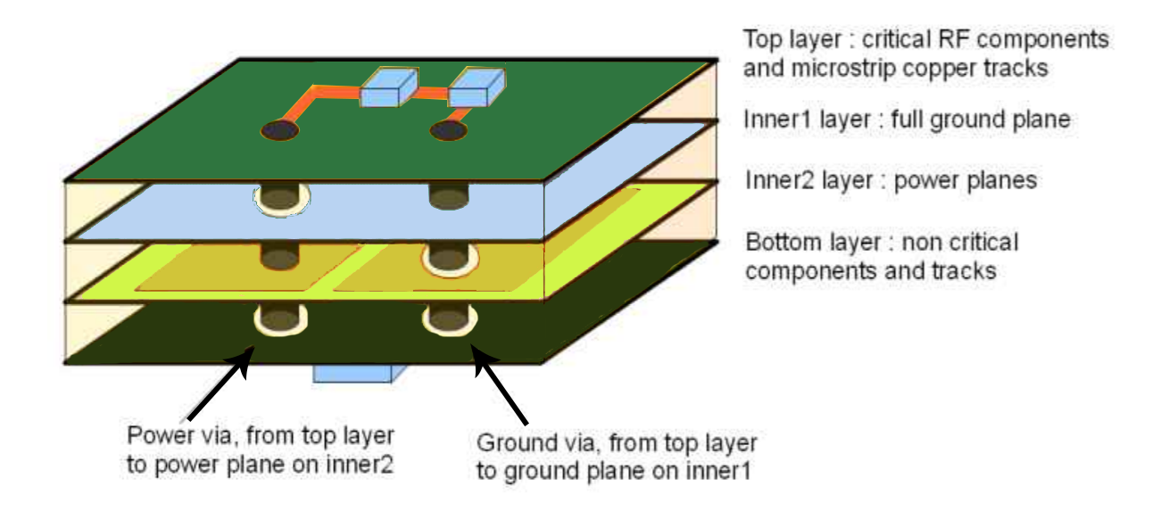
Using Vias Strategically in Multilayer Designs
Vias are essential in the multilayer PCB but can introduce signal discontinuities. Minimize via count by optimizing layer transitions and place vias away from high-speed signal paths when possible. Use back-drilling for unused via stubs to eliminate reflections. Surround critical vias with ground vias to provide a return path and reduce inductance. Standards like IPC-A-600K on acceptability of printed boards offer insights into via placement and quality that impact high-frequency performance.
Designing Effective Ground Planes for Stability
A solid ground plane is indispensable for high-frequency PCB routing. It provides a low-impedance return path for signals and shields against EMI. Avoid splitting ground planes under high-speed traces, as this disrupts return currents and increases interference. Ensure multiple ground vias connect planes across layers for uniform potential. Filling unused PCB areas with ground pours enhances shielding and heat dissipation. Guidelines from IPC-2221B emphasize the importance of continuous ground planes for signal integrity.
Additional Routing Considerations
Route high-frequency traces on outer layers whenever possible to minimize dielectric losses. Keep clock and high-speed signals away from board edges to avoid external interference. Use differential signaling for critical data paths to cancel out common-mode noise. These practices collectively reduce signal loss and enhance immunity to interference.
Common Challenges and Troubleshooting Tips
High-frequency PCB routing often presents challenges that require proactive troubleshooting. One frequent issue is impedance mismatch, leading to signal reflections. Engineers can address this by using simulation tools to verify trace impedance against design specifications before fabrication. Crosstalk due to insufficient trace spacing can be mitigated by rerouting traces or increasing board layers to provide more isolation. Ground plane discontinuities often cause EMI issues, which can be resolved by stitching ground planes with vias at regular intervals. If via-related signal degradation occurs, consider reducing via diameter or optimizing their placement. Adhering to acceptance criteria in IPC-A-600K ensures that manufacturing defects do not exacerbate routing issues. These troubleshooting steps, rooted in practical experience, help maintain signal integrity across diverse applications.
Conclusion
High-frequency PCB routing demands precision to minimize signal loss and interference in modern electronic systems. By focusing on trace length optimization, adequate trace spacing, strategic via usage, and robust ground plane design, engineers can significantly enhance signal integrity. These techniques, aligned with industry standards like IPC-2221B and IPC-6012E, provide a reliable framework for tackling the complexities of high-frequency designs. Implementing these best practices ensures that PCBs perform consistently in demanding environments, from telecommunications to automotive systems. As technology advances, staying informed about routing principles remains crucial for achieving optimal outcomes in every project.
FAQs
Q1: How does trace length affect signal loss in high-frequency PCB routing?
A1: Trace length impacts signal loss by increasing propagation delay and attenuation. Longer traces lead to higher resistance and potential reflections if impedance is not matched. Following standards like IPC-2221B, engineers should minimize trace lengths and use controlled impedance to ensure signal integrity at high frequencies.
Q2: What is the ideal trace spacing to prevent interference in PCB designs?
A2: Ideal trace spacing for high-frequency signals is typically three times the trace width to minimize crosstalk. This separation reduces electromagnetic coupling between adjacent traces. Adhering to IPC-6012E guidelines helps ensure spacing meets performance needs while avoiding interference in critical designs.
Q3: How can ground planes reduce EMI in high-frequency PCB routing?
A3: Ground planes provide a low-impedance return path for signals, reducing EMI by shielding traces from external noise. Continuous planes prevent ground loops and enhance stability. Stitching with vias, as recommended in IPC-2221B, ensures uniform potential and minimizes interference in high-frequency applications.
Q4: Why are vias a concern in high-frequency PCB designs for signal integrity?
A4: Vias introduce discontinuities that can cause signal reflections and parasitic inductance. Minimizing via count and using ground vias nearby helps maintain a return path. Following IPC-A-600K standards for via placement ensures manufacturing quality and reduces signal loss in multilayer designs.
References
IPC-2221B — Generic Standard on Printed Board Design. IPC, 2012.
IPC-6012E — Qualification and Performance Specification for Rigid Printed Boards. IPC, 2020.
IPC-A-600K — Acceptability of Printed Boards. IPC, 2020.


