Introduction
In RF PCB design, high-layer-count stackups present unique challenges due to the need for integrating complex digital, analog, and RF signals within compact form factors. As frequencies climb into the GHz range, PCB signal loss becomes a critical factor that can degrade performance, increase noise, and compromise system reliability. Effective stackup planning minimizes these losses by optimizing layer arrangement, material choices, and transmission line configurations. Electrical engineers must balance routing density with signal integrity to ensure low insertion loss and controlled impedance. This article explores structured approaches to high-layer-count stackups tailored for RF applications, drawing on engineering principles to guide design decisions. By focusing on high-frequency PCB materials and precise layering, designers can achieve superior RF performance.
Understanding High-Layer-Count Stackups in RF Applications and Why They Matter
A high-layer-count PCB stackup refers to the vertical arrangement of conductive copper layers separated by dielectric materials, typically exceeding 12 layers to accommodate dense interconnects in modern RF systems. In RF applications, such as radar, 5G base stations, and satellite communications, these stackups must support microstrip and stripline transmission lines while isolating sensitive RF signals from digital noise. Poor stackup design leads to increased PCB signal loss through crosstalk, reflections, and radiation, directly impacting receiver sensitivity and transmitter efficiency. Engineers prioritize symmetric stackups to prevent warpage and maintain consistent dielectric thicknesses across layers. The relevance intensifies with rising layer counts, where via transitions multiply and exacerbate losses if not managed. Ultimately, a well-planned stackup ensures impedance matching over wide bandwidths, vital for high-frequency operations.
Key Mechanisms of PCB Signal Loss in High-Frequency RF Designs
PCB signal loss in RF designs arises primarily from conductor losses, dielectric losses, and radiation losses, each amplified at high frequencies. Conductor losses stem from skin effect, where current flows near the copper surface, and surface roughness scatters signals, increasing attenuation proportionally with frequency squared. Dielectric losses occur as the insulating material absorbs energy, quantified by the loss tangent (Df), converting signal power to heat. Radiation losses happen when traces act as antennas, particularly at discontinuities like bends or vias, leaking energy into the substrate. In high-layer-count boards, via stubs and inter-layer transitions compound these effects, demanding careful stub management. Understanding these mechanisms allows engineers to target stackup features that suppress loss mechanisms effectively.
High-frequency PCB materials play a pivotal role in mitigating dielectric losses, as materials with low Df values preserve signal amplitude over long traces. Conductor losses demand smooth copper profiles and wider traces where possible, though layer density constrains options. Radiation is curtailed by embedding RF signals between ground planes, forming shielded striplines that confine fields.
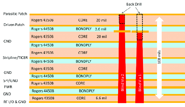
Related Reading: Core Thickness for RF PCBs: Minimizing Signal Loss in Wireless Applications
Selecting High-Frequency PCB Materials for Low Signal Loss
Choosing high-frequency PCB materials centers on dielectric constant (Dk) stability and minimal Df to curb PCB signal loss. Low Dk materials reduce phase velocity variations and support compact layouts, while low Df ensures less energy dissipation, especially above 1 GHz. Engineers evaluate materials for thermal stability, as CTE mismatches in multilayer stackups cause reliability issues under RF power. Hybrid stackups combine low-loss cores for RF layers with cost-effective prepregs for digital sections, optimizing overall performance. Material selection must align with fabrication capabilities to avoid voids or delamination that introduce additional losses. Consistent Dk across frequencies prevents impedance drifts, crucial for broadband RF PCB design.
In practice, cores with Df below 0.005 at 10 GHz suit demanding RF applications, paired with thin prepregs for tight layer control. Engineers verify material datasheets for frequency-dependent properties before stackup planning.
Stackup Design Strategies to Minimize Signal Loss in High-Layer-Count RF PCBs
Optimized RF PCB design begins with placing RF signal layers adjacent to ground planes, creating striplines with low radiation and controlled characteristic impedance. Symmetric stackups, such as 1-6-10 or mirrored configurations, distribute copper symmetrically to minimize bow and twist, adhering to IPC-2221 guidelines for layer sequencing. Thin dielectrics between signal and reference planes reduce mode conversion and loss, targeting 3 to 5 mil separations for GHz signals. Power planes should be dedicated and stitched to ground via arrays to form low-inductance returns, suppressing simultaneous switching noise that couples into RF paths. Via optimization, including blind and buried types, limits stub lengths to fractions of the signal wavelength, curbing reflections.
For high-layer counts above 20, dedicate inner layers to RF microstrips flanked by grounds, reserving outer layers for low-speed signals. Impedance control demands field solver verification during stackup finalization.
Breakout routing at BGA sites requires fanout with short vias, transitioning RF nets smoothly to inner layers. Ground pour continuity across planes via dense stitching vias further shields against EMI.
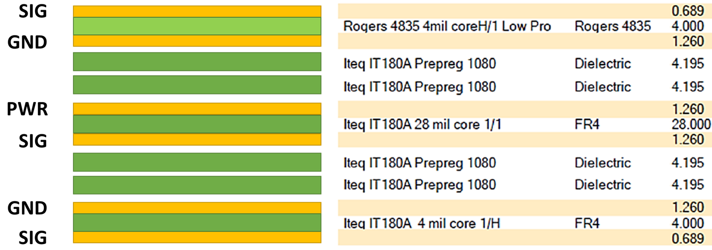
Reltaed Reading: High Frequency PCB Routing Techniques: Minimizing Signal Loss and Interference
Best Practices for Implementation and Verification
Practical RF PCB design incorporates field simulations early to predict insertion loss and return loss across the stackup. Engineers calculate effective Dk for mixed dielectrics and adjust trace widths for 50-ohm lines, iterating until losses stay below 1 dB per inch at operating frequencies. Fabrication tolerances, per IPC-6012 performance specs, influence dielectric thickness control, so specify tight tolerances for high-frequency layers. Thermal management integrates heat spreaders or embedded coins without disrupting RF fields. Post-layout reviews focus on via fence placement around RF sections to enhance isolation.
Assembly considerations include handling low-loss materials sensitively to avoid contamination that raises Df. Qualification testing validates stackup integrity under IPC standards.
Case Study Insights: Refining a Multilayer RF Stackup
Consider a hypothetical 24-layer PCB for a phased-array radar module, where initial stackup showed 2.5 dB excess loss at 8 GHz due to distant ground references and high-Df prepregs. Redesign embedded RF layers L10-L13 between full ground planes with low-Df cores, halving dielectric spacing to 4 mils. Hybrid materials segregated RF from digital sections, while blind vias eliminated through-stubs on critical nets. Simulations confirmed loss reduction to under 0.8 dB/inch, with S-parameters meeting specs. Fabrication emphasized pressed stackups for uniformity, aligning with IPC-2221 design principles. This approach extended operational bandwidth by 30%, underscoring stackup's role in RF performance.
Conclusion
High-layer-count PCB stackup design for RF applications demands a holistic approach to minimize PCB signal loss through material selection, layer pairing, and verification. Prioritizing low-loss high-frequency PCB materials and ground-proximate signals forms the foundation of robust RF PCB design. Symmetric configurations and via strategies further enhance integrity in dense boards. Electrical engineers benefit from early simulations and standards adherence to navigate complexities. Implementing these practices yields reliable, high-performance RF systems ready for demanding environments.
FAQs
Q1: What are the primary causes of PCB signal loss in high-frequency RF designs?
A1: Conductor losses from skin effect and copper roughness, dielectric losses quantified by material Df, and radiation from unshielded traces and discontinuities are dominant. High-layer stackups add via and stub contributions. Mitigation includes stripline embedding between ground planes, selecting low-Df high-frequency PCB materials, and maintaining tight fabrication tolerances.
Q2: How do high-frequency PCB materials impact RF PCB stackup performance?
A2: Materials with low Dk and Df minimize phase shifts and energy dissipation, enabling longer traces with lower attenuation. Stable Dk and Df across frequency maintain controlled impedance in multilayer builds. Hybrid stacks dedicate premium low-loss laminates to RF layers while using cost-effective materials for digital sections, directly reducing the overall PCB signal loss budget.
Q3: What stackup strategies best minimize signal loss in high-layer-count RF boards?
A3: Place RF signals between adjacent ground planes for shielding and impedance control. Use symmetric layering to prevent warpage per IPC guidelines. Minimize via lengths with blind and buried vias, add dense ground stitching, choose thin dielectrics (about 3–5 mil), and specify smooth copper to lower conductor loss.
Q4: Why is symmetric stackup critical for high-layer RF applications?
A4: Symmetry balances copper distribution, reducing warpage and dielectric asymmetry that cause skew and impedance drift. It supports uniform plating and lamination, improving high-frequency performance. Consistent thicknesses across layers help maintain impedance targets, aligning with IPC-2221 guidance for reliable RF PCB design.
References
IPC-2221 — Generic Standard on Printed Board Design. IPC
IPC-6012E — Qualification and Performance Specification for Rigid Printed Boards. IPC
IPC-6018C — Qualification and Performance Specification for High Frequency (Microwave) Printed Boards. IPC


