Introduction
In high-voltage PCB design, mastering pcb trace spacing high voltage is essential for preventing electrical breakdown and ensuring reliable operation. Engineers face challenges when dealing with voltages exceeding 500 volts, where insufficient spacing can lead to arcing, flashover, or conductive anodic filamentation. This high voltage pcb design guide focuses on creepage and clearance distances pcb, the critical parameters that dictate minimum trace spacing. Proper implementation not only enhances safety but also supports compliance with industry standards. As electric engineers push designs toward higher power densities, understanding these spacings becomes a cornerstone of robust circuit performance. This article provides logical, structured explanations to guide your design process.
Understanding Creepage and Clearance: Why Minimum Trace Spacing Matters
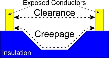
Creepage distance refers to the shortest path along the surface of the insulating material between two conductors, while clearance is the shortest air gap through the air between them. In high voltage pcb design guide contexts, these distances prevent dielectric breakdown, surface tracking, and corona discharge, which could compromise system integrity. For instance, at elevated voltages, electric field strength intensifies, risking partial discharges that degrade insulation over time. Industry relevance stems from safety certifications and operational reliability in power supplies, inverters, and electric vehicle electronics. Neglecting creepage and clearance distances pcb can result in field failures, increased manufacturing costs, or regulatory non-compliance. Engineers must prioritize these from the schematic stage to layout verification.
Minimum trace spacing for 1kv exemplifies the stakes, as spacings often exceed several millimeters depending on environmental factors. Pollution accumulation or humidity can bridge creepage paths, turning non-conductive surfaces conductive. Altitude affects clearance due to reduced air density, requiring larger gaps above 3050 meters. Material properties, such as comparative tracking index (CTI), further influence requirements. By adhering to standards like IPC-2221, designers mitigate these risks systematically. Ultimately, optimized spacing balances board real estate with performance margins.
Technical Principles of High-Voltage Trace Spacing
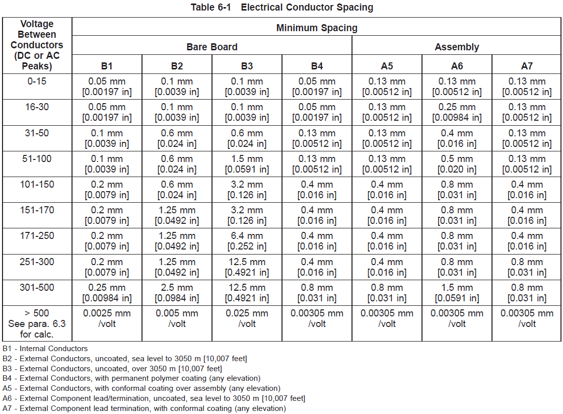
The core principle of pcb trace spacing high voltage revolves around voltage withstand capability, governed by Paschen's law for clearance and tracking resistance for creepage. Clearance scales with voltage because air breakdown voltage peaks around a 3 microns pressure-distance product but drops at extremes, demanding wider gaps for higher fields. IPC-2221B provides tabulated minimums for voltages up to 500 volts DC or peak AC, with external uncoated conductors at sea level requiring 2.5 mm for 301-500 volts in fabrication boards. Above 500 volts, add incremental values like 0.005 mm per volt for external uncoated traces, yielding approximately 5 mm at 1000 volts. Internal conductors need less, around 0.25 mm base plus 0.0025 mm per volt.
Creepage distances pcb vary by pollution degree, defined as 1 for clean environments, 2 for office settings with occasional condensation, and 3 for industrial dust. IEC 62368-1 tables specify, for example, 5.0 mm at 1000 volts RMS under pollution degree 2 and material group IIIa (CTI 175-400 volts). Material groups range from I (CTI over 600 volts) to IIIb (100-175 volts), with lower groups needing wider creepage. Coatings like solder mask or conformal coatings can reduce requirements by categorizing traces as protected. Altitude correction factors multiply clearance by 1.1 to 1.5 above 2000 meters. These mechanisms ensure the electric field stays below breakdown thresholds across operating conditions.
- Voltage: Increases linearly; peak AC or DC
- Pollution Degree: Higher degree widens creepage
- Material Group (CTI): Lower CTI requires more creepage
- Altitude: Multiplies clearance > 3050 m
- Coating: Reduces effective spacing needs
Practical Best Practices for High-Voltage PCB Layout
Implement net classes in your design software to enforce pcb trace spacing high voltage rules per voltage nets, overriding default clearances. Assign high-voltage nets to dedicated layers, routing them away from low-voltage signals with at least three times the trace width separation, known as the 3W rule. Use slots or grooves milled into the board to extend creepage paths without expanding footprint, effectively doubling distance along insulators. For minimum trace spacing for 1kv, verify against IPC-2221B calculations: external uncoated at sea level approaches 5 mm, but conformal coating drops it per table A5/A7 columns. Barrier ribs or potting compounds provide additional insulation for extreme cases.
Select FR-4 with high CTI (group II or better) for creepage reliability, and opt for thinner dielectrics cautiously to avoid field crowding. Perform design rule checks (DRC) for both clearance and creepage, simulating 3D paths around components. Test prototypes with high-potential (HiPot) at 1.5 to 2 times working voltage, monitoring for corona via UV detection. Iterate layouts to minimize vias under high-voltage traces, as they concentrate fields. Document assumptions like pollution degree 2 for regulatory audits. These steps ensure manufacturability and field durability.
Troubleshooting Common High-Voltage Spacing Issues
Engineers often encounter partial discharge in prototypes, indicated by ozone smell or erratic operation under load. This signals insufficient clearance; measure with a microscope and compare to IPC-2221B external columns, adjusting for altitude if applicable. Dendritic growth from ionic contamination shortens creepage over time, especially in humid environments, mitigated by no-clean fluxes and baking before coating. Flashover during HiPot testing points to pollution degree mismatch; upgrade to degree 1 assumptions only for sealed enclosures.
Component leads demand wider spacing per assembly tables, as uncoated leads (A6/A7) require up to 1.5 mm at 301-500 volts. Simulate field gradients with 3D solvers to identify hotspots. Post-failure analysis via cross-sectioning reveals tracking paths, guiding redesigns. Always validate with standards to avoid recurrence.
Conclusion
Mastering minimum trace spacing in high-voltage PCB design hinges on distinguishing creepage from clearance and applying standards like IPC-2221B and IEC 62368-1 judiciously. Factors such as pollution degree, CTI, and coatings dictate precise values, with 1000-volt applications typically needing 3-7 mm depending on conditions. Practical routing, verification, and troubleshooting ensure safety and performance. Engineers benefit from structured net rules and simulations to optimize board space. Prioritizing these principles yields reliable, certifiable designs. Adopt this high voltage pcb design guide for your next project to elevate engineering outcomes.
FAQs
Q1: What is the minimum trace spacing for 1kV in PCB design?
A1: For 1000 volts, IPC-2221B suggests around 5 mm clearance for external uncoated conductors at sea level, calculated as 2.5 mm base plus 0.005 mm per volt above 500 volts. Creepage per IEC 62368-1 reaches 5.0 mm under pollution degree 2 and material group IIIa. Always confirm with full tables and design rules for your conditions.
Q2: How do creepage and clearance distances differ in high voltage PCBs?
A2: Clearance measures the air gap between conductors, focusing on dielectric breakdown, while creepage follows the insulator surface, addressing tracking. IPC-2221B tabulates clearance by voltage and coating, whereas creepage in IEC 62368-1 factors pollution degree and CTI. Both are critical for pcb trace spacing high voltage above 50 volts.
Q3: What role does pollution degree play in pcb trace spacing high voltage?
A3: Pollution degree 1 assumes clean air, allowing tighter creepage; degree 2 accounts for condensation, needing wider paths like 5 mm at 1000 volts per IEC 62368-1; degree 3 for conductive dust demands even more. Select based on end-use environment to prevent surface conduction.
Q4: What are key tips in a high voltage pcb design guide for trace spacing?
A4: Use voltage-based net classes, the 3W rule for parallel runs, and slots for extended creepage. Reference IPC-2221B for clearances and verify with HiPot testing. Coatings reduce requirements but require assembly checks.
References
[1] IPC-2221B — Generic Standard on Printed Board Design. IPC
[2] IEC 62368-1 — Audio/video, information and communication technology equipment - Part 1: Safety requirements. IEC


