In high-speed PCB designs, calculating the impedance of transmission lines is critical for ensuring signal integrity and minimizing issues like reflections or crosstalk. Whether you're working with microstrip, stripline, or coplanar waveguide configurations, understanding how to determine impedance can make or break your design. This guide will walk you through the essentials of PCB transmission lines impedance calculation, breaking down the process for various structures used in high-speed PCB layouts.
At its core, impedance calculation involves determining the characteristic impedance of a transmission line, which depends on the geometry of the trace, the dielectric properties of the PCB material, and the surrounding environment. In this detailed blog, we'll cover the importance of impedance control, the formulas and tools for microstrip impedance calculation, stripline impedance calculation, and coplanar waveguide impedance calculation, along with practical tips for high-speed PCB designs.
Why Impedance Matters in High-Speed PCB Designs
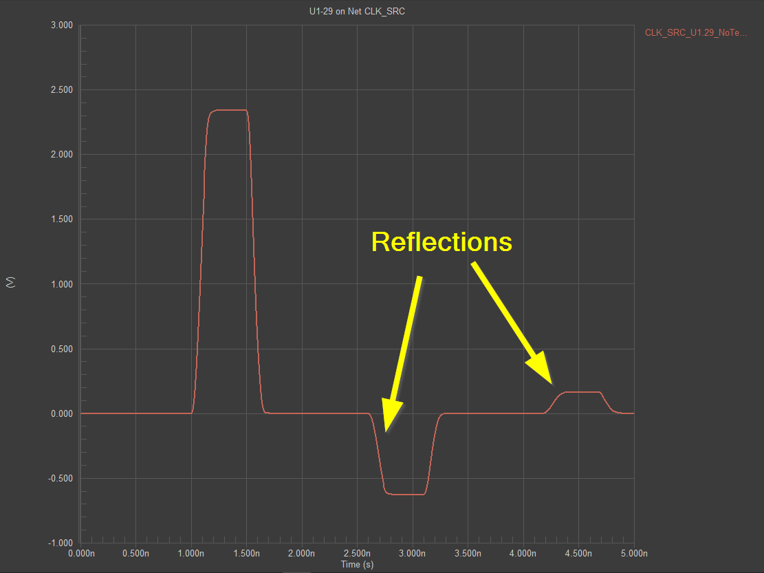
In high-speed PCB designs, signals travel at frequencies where transmission line effects become significant—often above 100 MHz. If the impedance of a trace isn't matched to the source and load, signal reflections can occur, leading to data errors, noise, or degraded performance. Proper impedance control ensures that signals propagate smoothly, maintaining their integrity over long traces or through complex layouts.
Impedance mismatches can cause issues like overshoot, ringing, or signal loss, especially in applications like USB, HDMI, or DDR memory interfaces. For instance, a common target impedance for many high-speed digital signals is 50 ohms for single-ended lines or 100 ohms for differential pairs. Achieving these values requires precise calculations based on the PCB stackup, trace dimensions, and material properties.
Understanding Transmission Lines in PCB Designs
Transmission lines on a PCB are conductive paths that carry high-frequency signals. The three most common types used in high-speed designs are microstrip, stripline, and coplanar waveguide. Each has unique characteristics and impedance calculation methods based on their physical structure and placement within the PCB layers.
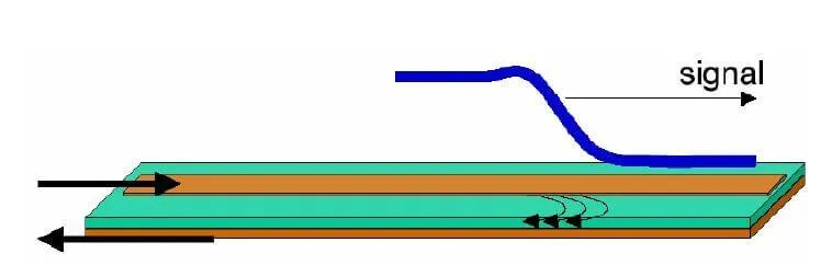
- Microstrip: A trace on the outer layer of a PCB with a ground plane beneath it. It's easy to fabricate but susceptible to external interference.
- Stripline: A trace embedded between two ground planes within the PCB. It offers better shielding but is harder to access for testing.
- Coplanar Waveguide (CPW): A trace on the outer layer with ground planes on either side on the same layer. It provides good isolation and is often used in RF designs.
Each of these structures requires a specific approach to calculate impedance, as their geometry and interaction with the dielectric material differ significantly.
Key Factors Affecting Impedance in PCB Transmission Lines
Before diving into calculations, it's important to understand the factors that influence impedance in PCB transmission lines. These include:
- Trace Width (W): Wider traces generally have lower impedance, while narrower traces have higher impedance.
- Trace Thickness (T): Thicker traces can slightly reduce impedance, though the effect is often minimal compared to width.
- Dielectric Height (H): The distance between the trace and the reference plane (ground) impacts impedance. A larger height increases impedance.
- Dielectric Constant (Er or Dk): The material property of the PCB substrate (like FR-4 with a typical Dk of 4.2-4.5) affects how much the electric field is slowed, influencing impedance.
- Trace Spacing (S): For differential pairs or coplanar waveguides, the spacing between traces or between trace and ground affects impedance.
These parameters are used in mathematical formulas or simulation tools to determine the characteristic impedance of a transmission line, typically measured in ohms.
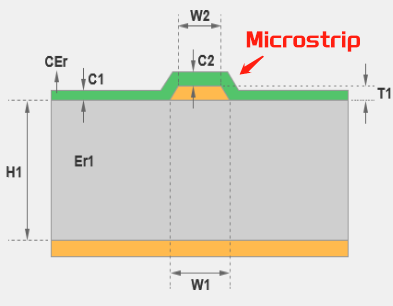
Microstrip Impedance Calculation for High-Speed PCB
Microstrip lines are widely used in high-speed PCB designs due to their simplicity and accessibility on the outer layers. The characteristic impedance of a microstrip can be calculated using the following approximate formula for a single-ended line:
Z0 = (87 / sqrt(Er + 1.41)) * ln(5.98 * H / (0.8 * W + T))
Where:
- Z0 is the characteristic impedance in ohms
- Er is the dielectric constant of the substrate
- H is the height of the dielectric (distance to ground plane) in mils or mm
- W is the trace width in mils or mm
- T is the trace thickness in mils or mm
For example, consider a microstrip on an FR-4 substrate with Er = 4.3, H = 10 mils, W = 6 mils, and T = 1.4 mils (typical for 1 oz copper). Plugging these values into the formula:
Z0 = (87 / sqrt(4.3 + 1.41)) * ln(5.98 * 10 / (0.8 * 6 + 1.4))
Z0 ≈ 50 ohms
This result shows that with these dimensions, the trace achieves the common 50-ohm impedance target for high-speed single-ended signals. However, for more accurate results, especially with complex stackups or higher frequencies, using a field solver or impedance calculator tool is recommended.
Stripline Impedance Calculation for High-Speed PCB
Stripline configurations, where the trace is sandwiched between two ground planes, offer better shielding and are often used in multilayer PCB designs. The impedance calculation for a stripline is slightly different due to the dual ground planes. The approximate formula for a single-ended stripline is:
Z0 = (60 / sqrt(Er)) * ln(4 * B / (0.67 * π * (0.8 * W + T)))
Where:
- Z0 is the characteristic impedance in ohms
- Er is the dielectric constant
- B is the total distance between the two ground planes in mils or mm
- W is the trace width in mils or mm
- T is the trace thickness in mils or mm
For instance, with Er = 4.3, B = 20 mils (10 mils above and below the trace), W = 5 mils, and T = 1.4 mils, the calculation yields:
Z0 = (60 / sqrt(4.3)) * ln(4 * 20 / (0.67 * 3.1416 * (0.8 * 5 + 1.4)))
Z0 ≈ 50 ohms
This matches the target impedance, but as with microstrip, real-world factors like manufacturing tolerances or frequency-dependent dielectric losses may require simulation tools for precision.
Coplanar Waveguide Impedance Calculation for High-Speed PCB
Coplanar waveguide (CPW) is often used in RF and microwave PCB designs due to its low radiation loss and ease of integration with surface-mount components. Calculating the impedance for CPW is more complex because it involves the spacing between the trace and the adjacent ground planes on the same layer. The formula for CPW impedance depends on whether it's a grounded or ungrounded configuration. A simplified approach for a grounded CPW uses numerical approximations or tools, but a rough formula is:
Z0 = (30 * π / sqrt(Er_eff)) / (K(k) / K(k'))
Where Er_eff is the effective dielectric constant, and K(k)/K(k') are elliptic integrals based on the ratio of trace width to gap spacing. Due to the complexity, most engineers rely on specialized calculators or simulation software for accurate coplanar waveguide impedance calculation.
For example, a CPW with a trace width of 10 mils, a gap of 5 mils on either side to the ground planes, and PCB FR4 material might target 50 ohms. Adjusting the gap or width in a calculator tool can help fine-tune the impedance to match design requirements.
Tools for Impedance Calculation in High-Speed PCB Designs
While manual calculations using formulas provide a good starting point, they often oversimplify real-world conditions like frequency dependence, manufacturing variations, or complex geometries. For high-speed PCB designs, using dedicated tools can save time and improve accuracy. Many online calculators and software solutions allow input of stackup details, trace dimensions, and material properties to predict impedance.
Some popular approaches include:
- 2D Field Solvers: These tools simulate the electromagnetic fields around a transmission line to compute impedance with high precision.
- PCB Design Software: Many design platforms integrate impedance calculators within their stackup editors, allowing real-time adjustments.
- Online Calculators: Free tools on the web can provide quick estimates for microstrip, stripline, and CPW impedances based on user inputs.
Using these tools ensures that your high-speed PCB design accounts for all variables, leading to better signal integrity and performance.
Practical Tips for Impedance Control in High-Speed PCB Designs
Beyond calculations, achieving the desired impedance in a high-speed PCB requires attention to design and manufacturing details. Here are some actionable tips:
- Choose the Right Material: Select a PCB substrate with a stable dielectric constant over the frequency range of your design. For instance, FR-4 works for many applications up to a few GHz, but high-frequency designs may need materials like Rogers or Isola.
- Maintain Consistent Trace Widths: Variations in trace width due to etching tolerances can alter impedance. Work with your manufacturer to ensure tight control over trace dimensions.
- Account for Differential Pairs: For differential signals, calculate the differential impedance (often 90-100 ohms) and ensure consistent spacing between the pair.
- Simulate at Target Frequencies: Impedance can vary with frequency due to skin effect or dielectric losses. Use tools to simulate behavior at your operating frequency, such as 1 GHz for DDR3 signals.
- Verify with Test Coupons: Include test structures on your PCB to measure actual impedance after fabrication, ensuring it matches your calculations.
Common Challenges in PCB Transmission Lines Impedance Calculation
Even with the best tools and formulas, challenges can arise in impedance control for high-speed PCB designs. Some common issues include:
- Material Variations: The dielectric constant of PCB materials can vary between batches, affecting impedance. Request detailed material datasheets from suppliers.
- Manufacturing Tolerances: Small deviations in trace width or dielectric thickness during fabrication can shift impedance. Typical tolerances for trace width might be ±10%, which could change a 50-ohm line to 48 or 52 ohms.
- Frequency Dependence: At very high frequencies, the skin effect and dielectric losses alter effective impedance. Always consider the frequency range of your signals.
Addressing these challenges requires collaboration with your PCB manufacturer and thorough simulation before finalizing the design.
Conclusion: Mastering Impedance for High-Speed PCB Success
Calculating the impedance of transmission lines is a fundamental step in high-speed PCB designs. Whether you're working with microstrip, stripline, or coplanar waveguide configurations, understanding the factors that influence impedance—trace dimensions, dielectric properties, and layout geometry—ensures signal integrity and reliable performance. By using the right formulas, tools, and design practices, you can achieve precise impedance control for your high-speed applications.
From microstrip impedance calculation to stripline and coplanar waveguide impedance calculation, the process may seem complex at first, but with practice and the right resources, it becomes a manageable part of PCB design. Focus on accurate stackup planning, leverage simulation tools, and maintain tight manufacturing controls to bring your high-speed PCB designs to life with confidence.


