Why Is Trace Width Important in High-Current PCB Design?
Designing printed circuit boards (PCBs) for high-current applications, such as those carrying 20 amps (20A), demands careful attention to trace width. An adequately sized trace is crucial for the PCB's reliability and operational safety. If a trace is too narrow for the current it needs to carry, its electrical resistance will cause excessive heat generation.
This overheating can lead to various problems, including degraded performance, delamination of the copper from the substrate, or even complete circuit failure. The primary goal in high-current PCB design is to ensure that trace dimensions allow the board to operate within safe temperature limits, thereby maintaining its long-term reliability and functionality.

What Factors Influence a PCB's Current Carrying Capacity?
Understanding how much current a PCB trace can safely handle before its temperature rises excessively is fundamental. This "current carrying capacity" is not a fixed value but rather depends on several interacting factors.
Key Determinants of Trace Capacity
● Copper Thickness: Typically measured in ounces per square foot (oz/ft²), common values are 1 oz (approximately 35 micrometers) and 2 oz (70 micrometers). A thicker copper layer provides more material for current flow, allowing it to carry more current for a given trace width without overheating.
● Trace Width: A wider trace inherently has lower resistance over a given length. This means it can dissipate heat more effectively and accommodate higher currents compared to a narrower trace of the same thickness.
● Permissible Temperature Rise: This refers to the maximum acceptable increase in the trace's temperature above the ambient environment. Common design targets are a 10°C, 20°C, or 30°C rise, depending on the application's sensitivity to heat and overall thermal budget.
● Layer Location (Internal vs. External): Traces on the outer layers (top or bottom) of a PCB can dissipate heat into the surrounding air more efficiently than traces embedded within internal layers. Consequently, external traces can often be narrower than internal traces for the same current capacity and temperature rise.
● Ambient Operating Temperature: If the PCB operates in a high-temperature environment, its ability to shed heat from the traces is diminished. This necessitates wider traces to maintain the same temperature rise limit.
For a design requiring 20A, each of these elements directly influences the minimum trace width necessary to ensure stable and safe operation.
How Are IPC-2221 Standards Used for Trace Width Calculations?
The IPC-2221 standard serves as a foundational reference for many aspects of PCB design, including guidelines for determining the appropriate trace width to safely carry a specified current. While more advanced standards like IPC-2152 exist, IPC-2221 remains widely utilized due to its established presence and relative ease of application.
The standard provides empirical data—typically in the form of charts or formulas—that illustrate the relationship between the current a trace carries, its copper thickness, and the resulting temperature rise. These guidelines are based on certain assumed conditions, such as a specified ambient temperature and the absence of forced airflow.
Applying IPC-2221 for a 20A Design
To calculate the trace width for a 20A circuit using IPC-2221, consider these steps:
● Identify the Current: Begin with the required current, which is 20A in this scenario.
● Specify Copper Thickness: Decide on the copper thickness. For high-current paths, 2 oz copper is frequently chosen over 1 oz due to its superior current handling and reduced width requirements.
● Set Temperature Rise Limit: Establish the maximum allowable temperature increase. A 10°C rise is a conservative choice, while 20°C or 30°C might be acceptable for less thermally sensitive applications.
● Determine Layer Position: Note whether the trace will be on an external (top or bottom) or internal layer, as external layers offer better heat dissipation.
● Consult IPC-2221 Data: Reference the IPC-2221 charts or use an online calculator based on these standards to find the corresponding trace width.
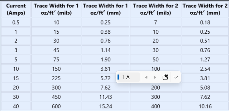
For instance, if you require 20A on an external layer using 1 oz copper with a maximum 10°C temperature rise, IPC-2221 suggests a trace width of approximately 5.2 mm (205 mils). If you increase the copper thickness to 2 oz under the same conditions, the required width significantly decreases to about 2.6 mm (102 mils), highlighting the impact of copper thickness on layout flexibility.
Step-by-Step Trace Width Calculation for a 20A Current
Let's walk through a practical example to determine the minimum trace width required for a 20A current on a PCB, using industry standards and typical design parameters.
Establishing Design Parameters
For this example, we'll define the following conditions:
● Target Current: 20 Amps (A)
● Copper Weight/Thickness: 2 ounces (oz), which is approximately 70 micrometers (µm)
● Maximum Temperature Rise: 10°C above ambient
● Trace Location: External layer (top or bottom)
● Ambient Temperature: 25°C
Calculating with IPC-2221 Data
Based on the IPC-2221 standard charts for external traces, a 20A current with 2 oz copper and a 10°C temperature rise necessitates a trace width of approximately 2.6 mm (or 102 mils). This dimension ensures the trace can safely conduct the current without exceeding the specified thermal limit.
Verifying with a PCB Trace Width Calculator
To minimize manual errors and save time, using an online PCB trace width calculator is highly recommended. These tools are typically built upon IPC-2221 or IPC-2152 data. By inputting the parameters (20A current, 2 oz copper, 10°C rise, external layer), most calculators will confirm the calculated 2.6 mm width, providing quick verification.
Adapting for Real-World Scenarios
The calculated width assumes ideal conditions. In practice, adjustments might be necessary:
● Elevated Ambient Temperature: If the PCB operates in a hotter environment (e.g., 40°C), or with restricted airflow, a wider trace may be needed to maintain the 10°C rise limit.
● Internal Layers: For traces routed on internal layers, where heat dissipation is less efficient, the width should be increased by roughly 50%. For instance, an internal 20A trace with 2 oz copper would require a width closer to 3.9 mm to achieve a similar 10°C temperature rise.
What Are Key Design Rules for 20A High-Current PCBs?
Beyond merely calculating trace width, designing types of PCBs for high currents like 20A involves adhering to a set of best practices to ensure long-term reliability and safety. These rules help manage thermal performance, minimize voltage drops, and maintain signal integrity.
Essential Guidelines for Robust High-Current Designs
● Utilize Thicker Copper: Whenever possible, specify copper weights of 2 oz or higher instead of the standard 1 oz. This significantly improves current-carrying capacity, often reducing the required trace width by nearly half for the same current, thereby saving valuable board space.
● Minimize Trace Lengths: Shorter high-current traces inherently have lower resistance. This reduces both the voltage drop across the trace and the amount of heat generated, making the power delivery more efficient. Route high-current paths as directly as possible between components.
● Employ Copper Pours or Planes: For extremely high currents, consider using large copper pours or dedicated power planes rather than individual traces. These larger copper areas distribute the current over a much broader surface, drastically lowering resistance and reducing localized heat buildup.
● Strategically Place Vias: Vias in high-current paths introduce additional resistance and can become hotspots. To mitigate this, use multiple vias in parallel, or larger diameter vias, to effectively spread the current and reduce resistance. For a 20A path, a single small via (e.g., 0.3 mm) is typically insufficient; several larger vias will be necessary.
● Ensure Adequate Spacing (Clearance): High currents often coincide with higher voltages. Maintain appropriate clearance (spacing) between high-current traces, as well as between traces and other components, to prevent arcing and ensure electrical isolation. IPC-2221 provides guidelines for spacing based on voltage levels.
● Integrate Thermal Management: If the PCB will operate in a confined enclosure, a high ambient temperature, or if a lower temperature rise is critical, implement active or passive thermal management solutions. This might include adding heat sinks to power components, incorporating thermal vias directly under components, or designing for forced airflow (fans).
● Consider Component Placement: Place high-current components strategically to minimize trace lengths and allow for better heat dissipation. Avoid routing sensitive signal traces too close to high-current paths to prevent electromagnetic interference (EMI).
By integrating these high-current PCB design rules, engineers can create boards that reliably handle 20A without succumbing to thermal stress or performance degradation.
Why Is 2 oz Copper a Preferred Choice for 20A Designs?
For PCBs designed to manage high currents like 20A, 2 oz copper often emerges as the preferred option among designers. This popularity stems from its optimal balance of performance, cost-effectiveness, and ease of manufacturing.
With 2 oz copper, the required trace width for a 20A current on an external layer (assuming a 10°C temperature rise) reduces to approximately 2.6 mm. This is a significant decrease compared to the 5.2 mm required for 1 oz copper under identical conditions. This reduction in width is crucial for compact designs where board space is at a premium.
Furthermore, 2 oz copper is a standard offering from the vast majority of PCB fabrication houses. It delivers clear thermal and electrical advantages over a 1 oz copper PCB without incurring the substantially higher costs or specialized manufacturing processes associated with thicker copper options such as 3 oz or 4 oz. Its improved heat dissipation also lowers the risk of thermal stress, making 2 oz copper a robust and widely adopted solution for high-current PCB designs.
Addressing Challenges in High-Current PCB Design
Designing a PCB capable of safely handling 20A presents several common challenges that require thoughtful solutions. Overcoming these hurdles is essential for a reliable and efficient final product.
Navigating Design Obstacles
● Space Limitations: The need for wider traces to carry high currents often clashes with the demand for compact board layouts. To manage this, consider using thicker copper (2 oz or more) to reduce the necessary trace width. Alternatively, a multi-layer board can help distribute high currents across several layers, effectively utilizing vertical space.
● Heat Management: High currents invariably generate heat. If this heat isn't effectively dissipated, it can lead to component damage and board failure. Implement strategies like incorporating thermal vias directly under heat-generating components, attaching heat sinks, expanding copper pours, or designing for active cooling (e.g., fans) if the operating environment is confined or has high ambient temperatures.
● Voltage Drop: Longer, higher-resistance traces can cause significant voltage drops, potentially affecting the performance of voltage-sensitive components. To mitigate this, keep high-current traces as short and direct as possible. Using thicker copper also reduces trace resistance, helping to maintain stable voltage levels across the board.
● Manufacturing Constraints: Extremely wide traces, very thick copper, or specialized thermal management features might push the limits of some PCB manufacturers' capabilities. It's crucial to consult with your chosen fabrication house early in the design process to understand their specific design rules and manufacturing tolerances.
Useful Tools and Resources for Trace Width Calculations
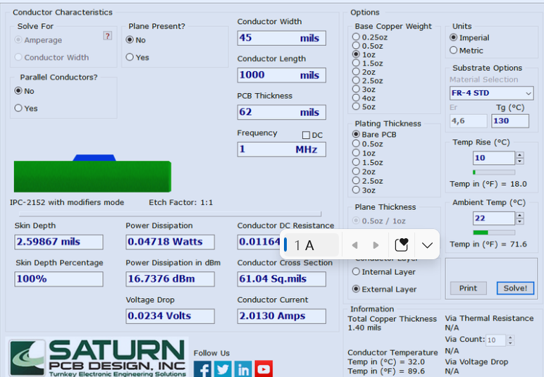
Manually calculating trace widths using IPC charts can be a time-consuming and error-prone process. Fortunately, various tools and resources are available to simplify and automate these calculations, ensuring accuracy and efficiency in your PCB design workflow.
Automated Calculation Tools
● Online PCB Trace Width Calculators: Numerous free online calculators are specifically designed to determine trace width based on IPC standards (such as IPC-2221 or IPC-2152). These tools typically require you to input parameters like the desired current (e.g., 20A), copper thickness, maximum allowed temperature rise, and whether the trace is internal or external. They instantly provide the recommended minimum trace width, saving significant time and reducing the chance of manual miscalculations.
● Integrated CAD Software Features: Most professional PCB design software packages (CAD tools) include built-in trace width calculators or design rule constraint managers. These features not only perform the calculations but can also automatically enforce the specified trace width rules during the board layout process. This integration helps maintain design integrity, especially for complex boards handling high currents.
These resources are invaluable for designers, allowing them to quickly and accurately determine appropriate trace widths, thereby enhancing the safety and reliability of their high-current PCB designs.
Concluding Thoughts on Designing High-Current PCBs
Successfully designing a PCB to handle a significant current like 20A demands a meticulous approach, focusing on trace width, copper thickness, and effective thermal management. By diligently adhering to industry standards such as IPC-2221 and leveraging specialized calculation tools, engineers can accurately determine the minimum trace dimensions required. For example, understanding that a 20A current on an external layer with 2 oz copper might necessitate a trace width of approximately 2.6 mm (for a 10°C temperature rise) is a critical starting point.
Implementing robust high-current PCB design rules—such as minimizing trace lengths, strategically employing copper pours, and carefully managing via placement—further bolsters the board's performance and longevity. Whether the application is in power electronics, automotive systems, or industrial control, a deep understanding of a PCB's current carrying capacity is non-negotiable. Prioritizing thicker copper, like 2 oz, often yields superior results, and always cross-referencing calculations with trusted standards or automated tools ensures both safety and efficiency in the final product.


