Introduction
The advent of 5G technology has transformed the landscape for electrical engineers, pushing the boundaries of PCB design to accommodate higher frequencies, faster data rates, and tighter performance constraints. Designing a 5G PCB layout requires meticulous attention to signal integrity, thermal management, and component placement to ensure optimal functionality. This article provides comprehensive guidelines for crafting effective 5G PCB layouts, focusing on best practices that align with industry standards. Aimed at electrical engineers, this content explores the technical nuances of 5G PCB design, offering actionable insights into layout strategies. Whether you are addressing high speed signal challenges or minimizing electromagnetic interference, these guidelines will equip you to navigate the complexities of modern PCB design for 5G applications.
What Is 5G PCB Design and Why It Matters
A 5G PCB refers to a printed circuit board engineered to support the stringent requirements of fifth generation wireless technology. Operating at frequencies up to 100 GHz in some bands, 5G systems demand PCBs that can handle high speed signals with minimal loss and interference. This technology is pivotal for applications like telecommunications, IoT devices, and autonomous systems, where latency and bandwidth are critical.
The importance of proper 5G PCB design cannot be overstated. Poor layout practices can lead to signal degradation, increased noise, and thermal issues, all of which compromise system performance. For electrical engineers, mastering these design principles ensures reliable operation of 5G enabled devices. Moreover, adhering to established guidelines reduces redesign cycles and enhances manufacturability, aligning with the fast paced deployment needs of 5G networks.
Technical Principles of 5G PCB Layout
Designing a PCB for 5G involves understanding several core principles that govern high frequency performance. At these elevated frequencies, even minor layout flaws can cause significant signal integrity issues. Below are the key technical aspects to consider during the design process.
High Frequency Signal Integrity
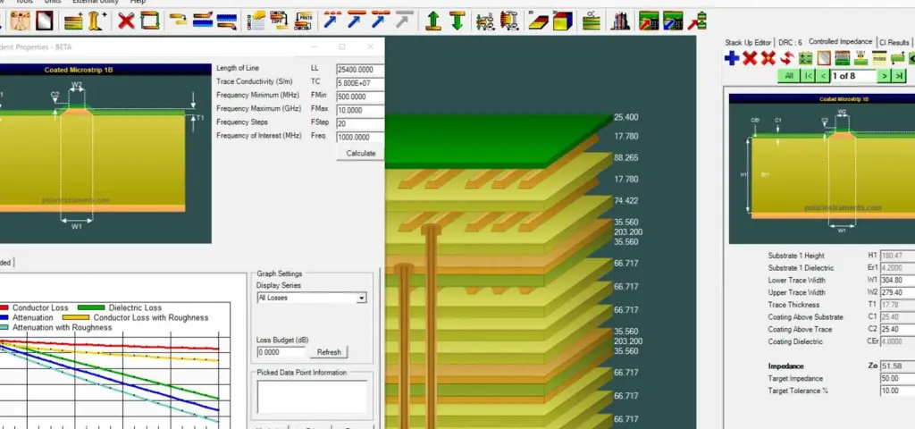
Signal integrity is paramount in 5G PCB design due to the short wavelengths involved. At millimeter wave frequencies, traces behave more like transmission lines, requiring controlled impedance to prevent reflections. Engineers must calculate trace widths and spacing based on the dielectric properties of the substrate to maintain consistent impedance. Additionally, minimizing via transitions and using smooth trace bends helps reduce signal loss.
Electromagnetic Interference Control
Electromagnetic interference becomes a critical concern as frequencies rise. Unshielded traces or poorly placed components can act as antennas, radiating unwanted noise. To mitigate this, grounding strategies such as continuous ground planes and strategic via stitching are essential. These techniques create a low impedance return path for high frequency currents, reducing interference.
Thermal Management Considerations
High speed 5G components often generate significant heat due to increased power densities. Without proper thermal management, reliability suffers, and performance degrades. Incorporating thermal vias, heat sinks, and adequate spacing around power intensive components helps dissipate heat effectively. Material selection also plays a role, as substrates with higher thermal conductivity improve heat transfer.
Practical Guidelines for 5G PCB Layout Design
Creating an effective 5G PCB layout demands a structured approach, integrating best practices with industry standards. These guidelines focus on actionable steps for electrical engineers to optimize their designs.
Component Placement Strategies
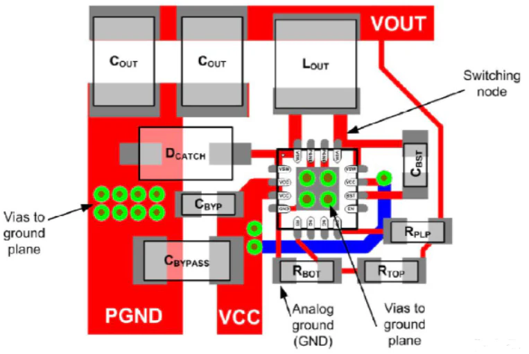
Component placement is the foundation of a successful 5G PCB layout. Place high frequency components close to their respective connectors to minimize trace lengths and reduce signal loss. Group related components together to streamline routing and avoid cross talk. Critical components like RF transceivers should be isolated from noisy digital circuits to prevent interference. Maintain symmetry in placement for differential pairs to ensure balanced signal propagation.
Trace Routing Best Practices
Routing traces for 5G PCBs requires precision to maintain signal integrity. Use shorter, direct paths for high speed signals, avoiding sharp corners that can cause reflections. Implement differential pair routing with consistent spacing to preserve signal timing. Keep traces over continuous ground planes to provide a stable return path. Adhering to standards like IPC-2221B helps define appropriate trace widths and clearances for high frequency designs.
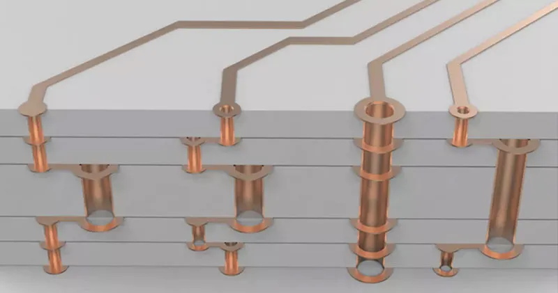
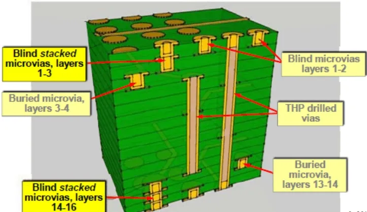
Layer Stackup Configuration
A well planned layer stackup is crucial for managing signal integrity and interference in 5G PCBs. Allocate dedicated layers for power and ground to minimize noise coupling. Place high speed signal layers adjacent to ground planes to control impedance and shield against interference. For complex designs, consider using more layers to segregate analog and digital signals, ensuring cleaner operation.
Suggested Reading: What is The Layer Stackup Design for optimum 5G Performance
Power Distribution Network Design
A robust power distribution network is vital to support the high current demands of 5G components. Use wide power traces or planes to reduce resistance and ensure stable voltage delivery. Place decoupling capacitors near power pins of active components to filter noise. Following guidelines from standards like IPC-2152 aids in designing power traces that handle current without excessive heating.
Grounding Techniques
Effective grounding is a cornerstone of 5G PCB design. Implement a solid ground plane beneath high frequency traces to provide a low impedance return path. Use multiple vias to connect ground planes across layers, reducing loop inductance. Avoid splitting ground planes under critical signal paths, as this can disrupt return currents and increase noise.
Addressing Common Challenges in 5G PCB Design
Even with careful planning, 5G PCB layouts often encounter challenges that require specific solutions. High frequency designs are prone to issues like cross talk, signal attenuation, and manufacturing constraints. Below are strategies to tackle these obstacles.
Minimizing Cross Talk
Cross talk occurs when signals from adjacent traces interfere with each other, degrading performance. To combat this, increase spacing between high speed traces as per guidelines in IPC-2221B. Use guard traces connected to ground between sensitive lines to absorb stray fields. Routing signals on different layers with intervening ground planes also helps isolate them.
Managing Signal Attenuation
Signal attenuation is a significant issue at 5G frequencies due to dielectric losses and skin effect. Select low loss materials with appropriate dielectric constants to reduce attenuation. Keep trace lengths as short as possible and avoid unnecessary vias, which introduce additional loss. Standards like JEDEC JESD204C provide insights into material selection for high speed applications.
Ensuring Manufacturability
Designing a 5G PCB that is manufacturable requires alignment with industry standards to avoid production issues. Tight tolerances for trace widths and via sizes must comply with specifications in IPC-6012E. Collaborate with fabrication teams early to confirm design rules, ensuring that the layout can be reliably produced without defects.
Conclusion
Designing a 5G PCB layout is a complex yet rewarding endeavor for electrical engineers. By focusing on signal integrity, component placement, and adherence to industry standards, engineers can create robust designs that meet the demands of high frequency applications. Implementing the guidelines discussed, from strategic trace routing to effective grounding, ensures optimal performance and reliability. As 5G technology continues to evolve, staying aligned with best practices and standards remains essential for success in this dynamic field.
FAQs
Q1: What are the key challenges in 5G PCB design?
A1: Designing a 5G PCB involves challenges like signal integrity at high frequencies, cross talk, and thermal management. Short wavelengths require precise impedance control and minimal trace lengths. Electromagnetic interference must be mitigated through proper grounding. Following standards like IPC-2221B helps address these issues with defined guidelines for trace spacing and layer configurations.
Q2: How does component placement affect 5G PCB performance?
A2: Component placement significantly impacts 5G PCB performance by influencing signal integrity and noise levels. Placing high frequency components near connectors reduces trace length and loss. Isolating RF parts from digital circuits prevents interference. Strategic placement ensures efficient routing and thermal dissipation, aligning with best practices for high speed design.
Q3: What standards should guide 5G PCB layout guidelines?
A3: For 5G PCB layout, standards like IPC-2221B for design rules and IPC-6012E for manufacturing specifications are crucial. JEDEC JESD204C offers material selection guidance for high speed signals. These standards provide frameworks for trace widths, clearances, and impedance control, ensuring reliability and performance in demanding 5G applications.
Q4: Why is grounding critical in 5G PCB layouts?
A4: Grounding is vital in 5G PCB layouts to provide a low impedance return path for high frequency signals. A continuous ground plane reduces noise and electromagnetic interference. Multiple vias connecting ground layers minimize loop inductance. Proper grounding, as outlined in IPC-2221B, ensures signal stability and enhances overall system performance.
References
IPC-2221B — Generic Standard on Printed Board Design. IPC, 2012.
IPC-6012E — Qualification and Performance Specification for Rigid Printed Boards. IPC, 2020.
JEDEC JESD204C — Serial Interface for Data Converters. JEDEC, 2017.