Introduction
Infotainment systems in modern vehicles integrate displays, audio processing, navigation, connectivity interfaces, and advanced driver assistance features into compact electronics. These systems demand printed circuit boards that handle high-speed signals like Ethernet, LVDS, and USB while managing significant power distribution for backlights and amplifiers. Multi-layer PCBs provide the necessary routing density, signal integrity, and electromagnetic compatibility required for reliable performance in harsh automotive environments. Designing such boards involves careful multi-layer PCB stackup design to balance impedance control, thermal management, and manufacturability. Engineers must address challenges like crosstalk, power integrity, and mechanical stability from vibration and temperature cycling. This article outlines structured approaches to via placement techniques, power and ground plane design, and layer transition optimization PCB strategies tailored for infotainment applications.
Fundamentals of Multi-Layer PCB Stackup Design for Infotainment Systems
Multi-layer PCB stackup design refers to the arrangement of copper layers, dielectrics, and planes that form the board's cross-section. For infotainment systems, stackups typically range from 8 to 16 layers to accommodate dense routing for high-speed differential pairs and multiple voltage rails. A well-planned stackup minimizes signal distortion by placing signal layers adjacent to reference planes, ensuring consistent impedance and low crosstalk. Core materials with low dielectric constant and loss tangent, such as those specified in industry guidelines, support frequencies up to several gigahertz common in video streaming and wireless modules.
Symmetry in the stackup prevents warpage during fabrication and assembly, with equal dielectric thicknesses on both sides of the core. Engineers prioritize ground planes as primary references for outer signal layers to create stripline or microstrip configurations with controlled characteristic impedance. Power planes should pair closely with ground planes to form low-inductance capacitance for power distribution networks. IPC-2221 provides foundational guidelines for layer sequencing, trace spacing, and material selection in such designs. Pre-production stackup verification through simulation confirms electrical performance before committing to fabrication.
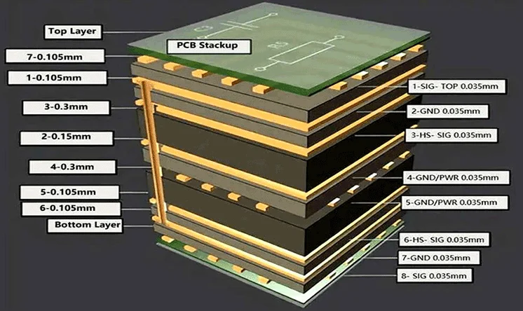
Routing high-speed interfaces requires dedicating inner layers to broadside-coupled pairs, avoiding splits in reference planes under critical traces. Thermal vias and embedded resistors may integrate into the stackup for heat dissipation from processors. Final stackup decisions balance cost, lead time, and performance, often iterating based on signal integrity simulations.
Essential Via Placement Techniques in Multi-Layer Designs
Via placement techniques critically influence signal integrity and board reliability in multi-layer PCBs for infotainment. Through-hole vias connect all layers but introduce stubs that cause reflections at high frequencies, so blind and buried vias reduce length for better performance. Strategic placement minimizes via-to-via coupling by maintaining clearances greater than three times the via diameter. For differential pairs, matched via pairs ensure symmetry, with ground vias nearby to contain return currents.
Stitching vias tie power and ground planes together, placed at intervals along splits or edges to lower impedance and enhance EMI shielding. Density rules limit via farms under BGAs to avoid drill breakout, favoring via-in-pad for high-density areas with filled vias for planarity. Engineers optimize via placement by grouping them near power pins for decoupling capacitors, reducing loop inductance. Simulations guide annular ring sizes to prevent drill wander in high-aspect-ratio boards.
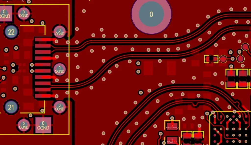
Laser-drilled microvias enable finer pitch escapes in HDI-style stackups common for compact infotainment modules. Post-placement checks verify no vias encroach on high-current paths, preserving thermal relief. These techniques collectively enhance yield and functionality.
Power and Ground Plane Design for Optimal Performance
Power and ground plane design forms the backbone of power integrity in multi-layer PCBs for infotainment systems. Dedicated full ground planes on inner layers provide return paths with minimal inductance, adjacent to signal layers for tight coupling. Power planes distribute multiple rails like 12V for displays and 3.3V for logic, segmented to isolate noisy digital supplies from analog audio circuits. IPC-2152 offers guidance on plane thickness for current-carrying capacity, preventing hotspots.
Plane splits require stitching vias every few millimeters to maintain continuity and reduce slot radiation. Decoupling capacitors bridge planes near ICs, with via pairs directly under pins for shortest paths. Wide spokes connect power pins to planes, minimizing voltage droop during transients. Ground planes act as shields, poured solidly except for clearance cutouts around high-voltage traces.
Hybrid planes combining power and ground through voltage partitioning save layers but demand careful simulation to avoid resonance. Plane resonance analysis ensures stable PDN impedance below 10 milliohms up to target frequencies. These practices sustain clean power delivery amid dynamic loads.
Layer Transition Optimization PCB Strategies
Layer transition optimization PCB techniques mitigate signal degradation in dense multi-layer boards. Backdrilling removes unused via stubs, critical for signals transitioning multiple layers in infotainment routing. Controlled depth drilling aligns with stackup thicknesses, verified by x-ray inspection. Staggered vias chain blind segments, shortening total length for gigabit speeds.
Transition zones avoid plane splits, using fanouts with minimal jogs. Microvia transitions stack two levels maximum per IPC guidelines to control capacitance. Optimization reduces insertion loss by 20 percent or more in simulations. Fanout patterns from fine-pitch packages use dogbone escapes for reliability.
Best Practices and Standards Compliance
Integrate DFM early by adhering to IPC-6012 qualification specs for rigid boards, ensuring plating uniformity and bow/warp limits. Simulate full stackup for crosstalk and eye diagrams before layout freeze. Prototype testing validates EMI with ground pours unbroken. Layer pairing evolves iteratively for balance.
Conclusion
Effective multi-layer PCB design for infotainment hinges on precise stackup planning, thoughtful via strategies, robust plane configurations, and seamless transitions. These elements ensure signal fidelity, power stability, and manufacturability. Engineers applying these principles deliver reliable systems meeting automotive demands.
FAQs
Q1: What are the key elements of multi-layer PCB stackup design for high-speed infotainment signals?
A1: Multi-layer PCB stackup design prioritizes signal layers next to ground planes for impedance control, symmetric dielectric stacks to prevent warpage, and low-loss materials for minimal attenuation. Pair power planes closely with grounds for capacitance. Simulate to target 50 or 100 ohm differentials. This setup supports Ethernet and video interfaces reliably.
Q2: How do via placement techniques impact power integrity in infotainment PCBs?
A2: Via placement techniques like stitching connect planes effectively, reducing PDN impedance, while blind vias shorten paths for high-speed nets. Place them densely near loads but avoid clusters causing thermal issues. Matched pairs maintain balance. Proper techniques minimize droop and noise in dynamic environments.
Q3: Why is power and ground plane design crucial in multi-layer PCBs for vehicles?
A3: Power and ground plane design provides low-inductance distribution, shielding signals from EMI, and stable references. Segment planes for isolation, stitch splits, and decouple aggressively. This sustains performance under vibration and temperature swings in infotainment.
Q4: What strategies improve layer transition optimization PCB in dense designs?
A4: Layer transition optimization PCB uses backdrilling and microvias to eliminate stubs, staggered chaining for length control, and clear transition zones. Verify depths and simulate losses. These reduce reflections for clean high-speed eyes.
References
IPC-2221 — Generic Standard on Printed Board Design. IPC
IPC-6012E — Qualification and Performance Specification for Rigid Printed Boards. IPC, 2017
IPC-2152 — Standard for Determining Current Carrying Capacity in Printed Board Design. IPC.