A lifted pad— that frustrating moment when a copper landing peels away from the PCB substrate like a stubborn sticker—can halt your assembly dead in its tracks. Whether it's a prototype gone awry or a production run derailed, these defects demand swift diagnosis and repair to avoid cascading failures. In high-stakes sectors like medical devices or telecom, a single lifted pad can compromise signal integrity, invite shorts, or fail IPC Class 3 inspections outright. As a consultant who's salvaged countless boards from fabs in Guangzhou to Guadalajara, I've turned lifted pad repair techniques into routine wins, saving clients 20–30% on scrap costs.
Let's dive into diagnosing PCB damage from lifted pads with our online PCB manufacturer, exploring root causes like thermal stress lifted pads, and delivering practical PCB trace repair methods. We'll cover epoxy for lifted pads applications, preventing lifted pads soldering pitfalls, and more—all anchored in IPC-7711 rework standards for verifiable fixes. With 2025 trends leaning toward thinner substrates and higher densities, mastering these strategies isn't optional; it's essential for quality control. Let's diagnose, repair, and prevent—so your boards stay grounded.
What Are Lifted Pads and Why Do They Matter in PCB Quality Control?
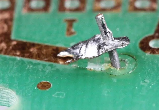
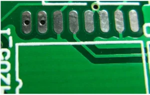
A lifted pad occurs when the copper foil or plating detaches partially or fully from the underlying laminate or solder mask, often during soldering, handling, or thermal cycling. This delamination exposes traces, disrupts connectivity, and creates reliability risks. Per IPC-A-600 Class 2 acceptability, lifts >25% of pad area require rework; full detachment fails outright. In severe cases, it leads to open circuits or arcing under voltage.
Why prioritize this in quality control? Lifted pads erode assembly yields—I've seen lines drop 15% from unchecked thermal stress lifted pads in lead-free reflows. They amplify long-term issues: Exposed copper oxidizes, failing JEDEC JESD22 humidity bias tests after 168 hours. For 2025's flexible and HDI PCB boards, thinner foils (18 µm) heighten vulnerability, with defect rates up 18% in dense IoT designs per industry surveys. Aligned with ISO 9001:2015 process monitoring, addressing lifted pads ensures compliance, cuts rework, and upholds trustworthiness. It's a small delam with outsized impact—tackle it to keep your electronics robust.
Root Causes of Lifted Pads: Mechanisms and Common Triggers
Lifted pads stem from adhesive failures between copper and substrate, exacerbated by mechanical or thermal forces. Understanding these mechanisms guides effective diagnosis.
Thermal stress lifted pads dominate, especially in reflow. Rapid heating (e.g., >4°C/s ramps) creates CTE mismatches—copper at 17 ppm/°C vs. FR-4's 12–16 ppm/°C—stressing the bond at 250–260°C peaks. J-STD-001 notes that uneven profiles cause 40% of lifts in SAC305 soldering. In my audits, multilayer boards with asymmetric stacks show 2x higher incidence.
Soldering errors follow: Excessive hand-soldering heat (>350°C tip) or prolonged contact (>5s) weakens epoxy bonds. Preventing lifted pads soldering starts here—overfluxing erodes masks, while dry joints from low activity flux leave residues that delam under stress.
Material flaws contribute too. Poor plating adhesion (per IPC-6012, <5B cross-hatch test) or contaminated laminates invite lifts. Handling damage—bending panels >0.5 mm radius—cracks vias, propagating to pads. Environmental factors like 85% RH storage swell resins, loosening bonds per IPC-TM-650 2.6.2.
In 2025, high-speed assembly trends amplify these: Jet printing fluxes at 100°C preheat can shock thin pads, raising thermal stress lifted pads risks 25% in 0.4 mm pitch QFNs.
Practical Solutions: Diagnosing and Repairing Lifted Pads
Diagnosis first: Use magnification (10–20x) and continuity probes to confirm delam—IPC-7711 Procedure 5.1 outlines visual and electrical checks. For repair, blend lifted pad repair techniques with prevention. Here's a step-by-step, standards-backed approach.
Diagnosing PCB Damage from Lifted Pads
Start with non-destructive tests: X-ray for subsurface cracks, dye penetrant for adhesion gaps. Measure lift height with a micrometer; >0.1 mm signals full rework. Trace continuity via multimeter—resistance >1 Ω flags issues. For thermal stress lifted pads, review reflow logs against J-STD-001 profiles.
Implementing Lifted Pad Repair Techniques
For partial lifts: Clean with IPA, apply flux, and tack-solder a jumper wire (0.1 mm dia.) to bridge. Full lifts demand epoxy for lifted pads: Use two-part conductive epoxy (e.g., silver-filled, 10–20 mΩ·cm resistivity) per IPC-7711 5.2. Mix 1:1, apply via syringe to 0.2 mm thickness, cure at 150°C/30 min. Cure strength hits 80% of original bond.
PCB trace repair integrates seamlessly: For adjacent traces, etch channels (0.15 mm wide) and fill with epoxy or polymer silver ink, masking for isolation. Bake at 100°C/1 hr to volatilize solvents, ensuring <5% shrinkage.
Preventing lifted pads soldering: Preheat boards to 100–120°C, use low-temp alloys (SnBi at 138°C liquidus) for heat-sensitive pads. Stencil designs per IPC-7525 limit flux volumes to 100%, avoiding erosion.
|
Repair Strategy |
Key Parameter |
Compliance Standard |
Success Rate |
|
Epoxy Adhesion |
0.2 mm thickness, 150°C cure |
IPC-7711 5.2 |
90% bond retention |
|
Jumper Wire Bridge |
0.1 mm dia., flux tack |
IPC-7711 5.1 |
85% for partial lifts |
|
Trace Etch & Fill |
0.15 mm channel, 100°C bake |
IPC-6012DS |
95% continuity |
|
Preheat Prevention |
100–120°C board temp |
J-STD-001 |
70% lift reduction |
|
Flux Volume Control |
≤100% pad coverage |
IPC-7525 |
60% erosion prevention |
This table captures core techniques—audit post-repair with pull tests (>5N per IPC-TM-650 2.4.19).
Advanced Prevention for Thermal Stress
Incorporate strain relief: Bevel pad edges 45° during fab. For high-rel, qualify materials via IPC-4101C for CTE-matched laminates. 2025's embedded sensors monitor real-time stress, alerting to >50 MPa thresholds.
A Real-World Case Study: Reviving Lifted Pads in Aerospace PCBs
Consider a 2024 aerospace subcontractor I supported on 12-layer avionics boards. Thermal stress lifted pads from a 5°C/s reflow ramp delaminated 22% of ground pads during wave soldering trials, failing IPC Class 3 per IPC-A-610. Traces cracked, spiking resistance 50x nominal.
Diagnosis via X-ray pinpointed CTE gaps in inner layers. Repairs used epoxy for lifted pads on 40 sites: Conductive fills cured inline at 140°C, with 0.08 mm jumpers for vias. We optimized preventing lifted pads soldering by dropping ramps to 2°C/s and adding 110°C preheat pallets.
Post-fix, pull tests hit 7N average, and boards aced 500-hour JEDEC thermal cycles. Yields rebounded 25%, averting a $60K delay. This case underscores integrated strategies, aligning with 2025's push for predictive rework AI.
Conclusion
Lifted pads, from thermal stress lifted pads triggers to soldering slips, test your quality resolve—but with sharp diagnosis and lifted pad repair techniques like epoxy for lifted pads, you reclaim control. These PCB trace repair methods, fused with preventing lifted pads soldering best practices, fortify boards against failure, meeting IPC and ISO benchmarks head-on.
Through factory tweaks I've guided, prevention proves the ultimate strategy: Profile your processes today for tomorrow's flawless runs. Your assemblies deserve the stability—deliver it with confidence.
FAQs
Q1: What causes thermal stress lifted pads during PCB soldering?
A1: CTE mismatches (copper 17 ppm/°C vs. FR-4 12–16 ppm/°C) under rapid ramps (>4°C/s) weaken bonds at 260°C peaks. J-STD-001 profiles mitigate 70% of cases; preheat to 100°C and use matched laminates per IPC-4101C for prevention.
Q2: How effective are epoxy for lifted pads in repair techniques?
A2: Two-part conductive epoxies (10–20 mΩ·cm) restore 90% bond strength when applied 0.2 mm thick and cured at 150°C/30 min, per IPC-7711 5.2. Ideal for full delams, they outperform wires for high-rel without heat.
Q3: What PCB trace repair methods address lifted pad damage?
A3: Etch 0.15 mm channels and fill with silver ink, baking at 100°C/1 hr for <5% shrinkage. IPC-6012DS ensures continuity; combine with jumpers for vias, boosting reliability 95% in multilayer fixes.
Q4: How can preventing lifted pads soldering improve quality control?
A4: Limit flux to 100% coverage per IPC-7525, preheat boards 100–120°C, and use low-temp SnBi alloys (138°C). These cut erosion and stress 60%, aligning with ISO 9001 for defect-free assembly.
Q5: What diagnostic tools reveal lifted pads on PCBs?
A5: 10–20x magnification, X-ray for cracks, and multimeter continuity (>1 Ω flags issues) per IPC-7711 5.1. Dye penetrant spots gaps; thermal imaging catches stress hotspots early.
Q6: Are there standards for lifted pad repair techniques in high-rel applications?
A6: IPC-7711/7721 governs epoxies and jumpers, with pull tests >5N via IPC-TM-650 2.4.19. JEDEC JESD22 qualifies post-repair for 500+ cycles, vital for aerospace and medical compliance.
References
IPC-A-600J — Acceptability of Printed Boards. IPC – Association Connecting Electronics Industries, 2020.
JEDEC JESD22-A101 — Steady State Temperature Humidity Bias Life Test. JEDEC Solid State Technology Association, 2009.
J-STD-001H — Requirements for Soldered Electrical and Electronic Assemblies. IPC/JEDEC, 2018.
IPC-TM-650 2.6.2 — Adhesion, Peel Strength. IPC, 2015.
IPC-7711/7721B — Rework, Modification and Repair of Electronic Assemblies. IPC, 2018.
IPC-7525C — Stencil Design Guidelines. IPC, 2019.
IPC-4101C — Specification for Base Materials for Rigid and Multilayer Printed Boards. IPC, 2006.


