Introduction
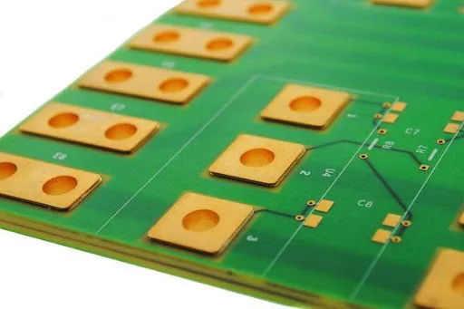
3 oz copper PCBs represent a critical advancement in printed circuit board technology, enabling higher current-carrying capacities and improved thermal dissipation in demanding applications. These boards feature copper layers approximately 105 micrometers thick, significantly heavier than the standard 1 oz copper at 35 micrometers. Electrical engineers specify 3 oz copper for power electronics, automotive systems, and industrial controls where standard thicknesses fall short. However, the PCB manufacturing process for such thick copper introduces unique hurdles that can compromise yield and reliability. This article explores these challenges in 3 oz copper PCB fabrication, etching, and assembly, while offering factory-proven solutions grounded in industry practices. By addressing these issues proactively, engineers can achieve robust boards that meet performance expectations.
What Are 3 oz Copper PCBs and Why They Matter
3 oz copper PCBs are defined by their copper foil weight of 3 ounces per square foot, translating to a nominal thickness of 105 micrometers per layer. This thickness supports elevated current densities without excessive heating, making them essential for high-power designs. In contrast to lighter copper weights, 3 oz layers reduce voltage drops and enhance mechanical strength in harsh environments. Electrical engineers value them in sectors like renewable energy inverters and electric vehicle power modules, where thermal management is paramount. The relevance stems from the growing demand for compact, high-reliability electronics that handle amperage levels beyond conventional boards. Yet, this thickness amplifies complexities throughout the PCB manufacturing process, necessitating specialized handling.
Factory insights reveal that 3 oz copper demands adjustments in nearly every fabrication step to maintain integrity. Without proper planning, issues like uneven material distribution can lead to failures under load. Engineers must balance performance gains against manufacturability trade-offs early in design.
Key Challenges in 3 oz Copper PCB Fabrication
Fabricating 3 oz copper PCBs begins with material preparation and lamination, where the thicker foil introduces stress imbalances. During pressing, differential expansion between copper and dielectric materials risks delamination or voids at interfaces. Thicker copper exacerbates these effects, as higher pressures are needed for adhesion, yet excessive force can cause resin starvation. Drilling presents further difficulties, with copper smearing or wrapping around hole walls due to the material's ductility. Plating high-aspect-ratio vias becomes uneven, as current distribution favors panel edges over centers. These fabrication hurdles directly impact subsequent steps like etching and assembly.
Warpage emerges as a pervasive issue from asymmetric stackups or unbalanced copper areas. Thick layers on one side pull the board during cooling, deviating from flatness tolerances. Misalignment between layers compounds this, as drilling inaccuracies propagate through multilayers. Factory experience shows that without mitigation, yield drops significantly in production runs.
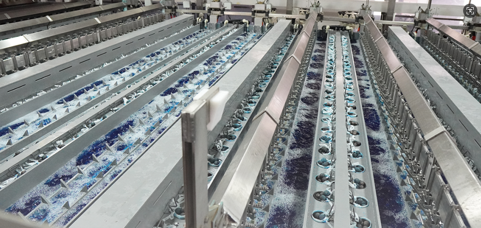
Challenges in 3 oz Copper PCB Etching
Etching 3 oz copper layers requires extended exposure to remove substantial material volume, heightening risks of underetching, overetching, and uneven profiles. Underetching leaves residual copper, creating shorts, while overetching narrows traces beyond design limits, reducing current capacity. Lateral etching, or undercutting, proves most problematic, as the isotropic process attacks sidewalls more aggressively in thicker foils. This demands precise compensation in artwork, often several mils per side, to achieve final trace widths. Uneven etching arises from etchant stagnation in dense patterns or warped boards, known as the pool effect, leading to inconsistent line widths.
Temperature gradients and spray inconsistencies amplify these defects in thick copper etching. Factory lines report doubled etching times compared to 1 oz boards, straining equipment and increasing defect rates. IPC-A-600 acceptability criteria become harder to meet, as surface roughness and edge definition suffer.
Challenges in 3 oz Copper PCB Assembly
Assembly of 3 oz copper PCBs faces thermal and mechanical strains from the hefty conductors. Soldering high-mass traces risks incomplete wetting or tombstoning due to rapid heat-up differences. Vias and pads plated over thick bases may exhibit voids if reflow profiles are not optimized. Component leads struggle with barrel fill in plated-through holes, especially under IPC-A-610 Class 3 scrutiny. Heavier boards also complicate handling, increasing handling-induced damage. PCB quality control during assembly detects these, but prevention starts upstream.
Practical Solutions for 3 oz Copper PCB Fabrication
To counter fabrication challenges, select laminates with high glass transition temperatures above 170 degrees Celsius for better adhesion and reduced delamination risk. Pre-bake panels to expel moisture before lamination, applying vacuum assistance for uniform resin flow. Balance copper distribution across layers using thieving patterns to equalize plating and etching loads. For drilling, employ high-precision machines with peck cycles to minimize burrs and copper wrap, followed by desmear processes tailored to thick foils. Pulse-reverse plating ensures uniform deposition in vias, targeting current densities around standard ranges for the aspect ratio.
Stackup simulation tools predict warpage, guiding symmetric designs with paired thick layers. Factory best practices include fiducial marks for alignment verification post-lamination. These steps align with IPC-6012 performance specifications for rigid boards.
Best Practices for 3 oz Copper PCB Etching
Optimize etching parameters by extending dwell times proportionally to thickness while monitoring etchant concentration and temperature within tight bands. Implement high-pressure multi-angle spray systems with regular nozzle maintenance to eliminate pool effects and ensure uniform flow. Design traces with widened dimensions and etching compensation, typically accounting for lateral loss, alongside minimum spacings to boost yield. Multiple etching passes may be necessary for 3 oz copper, interspersed with inspections. Incorporate copper balancing on panels to prevent density variations that cause uneven removal.
Agitation enhancements like ultrasonics or air sparging improve solution renewal over surfaces. Post-etch cross-sections verify sidewall integrity per IPC-A-600 guidelines. These measures maintain traceability and repeatability in production.
Solutions and Best Practices for 3 oz Copper PCB Assembly and Quality Control
For assembly, develop reflow profiles with extended preheats to equalize temperatures across thick copper planes. Incorporate thermal vias and pads to aid dissipation, reinforcing critical traces if needed. PCB quality control employs automated optical inspection for plating uniformity and X-ray for voids, alongside electrical testing for continuity. Warpage checks using dial gauges ensure compliance before assembly. J-STD-001 soldering standards guide barrel fill and defect limits.
Incorporate design for manufacturability by consulting fabricators early on trace routing and material choices. Prototype runs validate processes, iterating on stackups and profiles.
PCB Quality Control in Thick Copper Production
Rigorous quality control spans inline metrology for copper thickness post-plating and etch factor analysis. Electrical testing confirms resistance within specs, while thermal cycling simulates operational stress. Adhesion pull tests quantify layer bonds, flagging delamination risks. Documentation tracks process parameters, enabling root-cause analysis for defects. These controls uphold consistency across batches.
Conclusion
Manufacturing 3 oz copper PCBs demands meticulous attention to fabrication, etching, and assembly challenges like uneven etching, warpage, and plating defects. Factory-driven solutions, including balanced designs, optimized processes, and stringent quality control, mitigate these effectively. Electrical engineers benefit from wider traces, high-Tg materials, and precise parameter control to realize high-reliability boards. Adhering to standards ensures performance in power-intensive applications. Proactive planning yields superior outcomes, minimizing costs and rework.
FAQs
Q1: What are the primary challenges in 3 oz copper PCB etching?
A1: Thicker copper leads to prolonged etching times, increasing risks of underetching, overetching, and lateral undercutting that narrows traces. Uneven etchant flow causes pool effects in dense areas, compromising line uniformity. Solutions involve compensation in design, optimized spray systems, and balanced copper distribution for consistent results in the PCB manufacturing process.
Q2: How does warpage affect 3 oz copper PCB fabrication?
A2: Warpage arises from thermal mismatches and unbalanced copper, bending boards during lamination or cooling. This misaligns layers and hinders drilling accuracy. Mitigate with symmetric stackups, high-Tg dielectrics, and pre-baking, verified through quality control measurements to maintain flatness.
Q3: What best practices improve 3 oz copper PCB assembly?
A3: Tailor reflow profiles for even heating, add thermal vias for dissipation, and inspect for voids per assembly standards. Wider pads aid soldering on heavy traces. PCB quality control with AOI and X-ray ensures reliability in high-current applications.
Q4: Why is quality control critical in 3 oz copper PCB manufacturing?
A4: Thick copper amplifies defects like delamination and plating nonuniformity, impacting performance. Inline inspections, electrical tests, and process monitoring per IPC guidelines detect issues early. This sustains yield and meets engineering specs for demanding environments.
References
IPC-6012E — Qualification and Performance Specification for Rigid Printed Boards. IPC, 2017
IPC-A-600K — Acceptability of Printed Boards. IPC, 2020
IPC-A-610F — Acceptability of Electronic Assemblies. IPC, 2014


