Introduction
In the competitive landscape of electronics manufacturing, achieving PCB cost optimization requires careful consideration of every design element, particularly inner layer copper thickness. Engineers often face the challenge of balancing manufacturing expenses with electrical performance demands in multilayer boards. Inner layer manufacturing processes directly influence copper thickness cost, as thicker foils demand more resources during etching and lamination. Selecting the appropriate thickness supports cost-effective PCB design while ensuring reliability under operational stresses. This article explores the tradeoffs involved, drawing from factory-driven insights to guide technical professionals.
Copper thickness, typically measured in ounces per square foot, dictates material usage and processing complexity. Standard weights like 1 oz/ft2 equate to approximately 35 microns, forming the baseline for most designs. Deviating to heavier weights enhances performance but escalates costs across the production cycle. PCB material selection ties closely to these choices, as laminate compatibility and stackup symmetry play key roles. Understanding these dynamics empowers engineers to optimize without compromising quality.
Understanding Inner Layer Copper Thickness and Its Importance
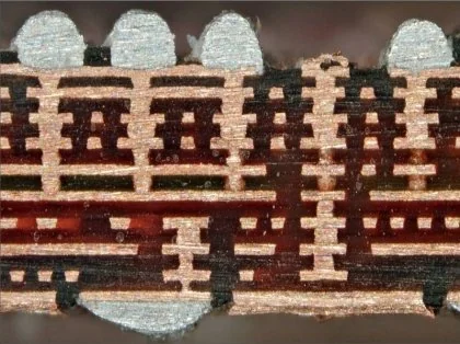
Inner layer copper thickness refers to the foil weight laminated between dielectric cores in multilayer printed circuit boards. Unlike outer layers, which may receive additional plating, inner layers rely on the initial foil thickness post-etching and oxide treatment. This thickness remains critical for power distribution, ground planes, and signal routing in dense designs. Factory processes treat inner layers differently, using reverse-treated foils to promote adhesion during multilayer pressing.
The relevance stems from multilayer PCBs dominating high-performance applications, where inner layers handle substantial current loads. Thicker copper improves thermal dissipation and reduces resistance, vital for power integrity. However, it complicates inner layer manufacturing due to etching challenges and potential warpage. PCB cost optimization hinges on specifying only the necessary thickness, avoiding overdesign that inflates expenses. As boards grow complex, precise selection prevents yield losses from misalignment or delamination.
Industry standards like IPC-6012 outline minimum finished copper thicknesses for internal layers, ensuring consistency across production runs. These guidelines account for process reductions during etching and lamination. Engineers must align designs with such specifications to maintain acceptability criteria. Neglecting this balance risks performance shortfalls or unnecessary copper thickness cost premiums.
Technical Principles Governing Copper Thickness Selection
Copper thickness selection begins with electrical requirements, particularly current-carrying capacity. IPC-2221 provides design guidelines for conductor sizing, differentiating internal layers from external due to differing heat dissipation. Internal traces experience reduced convection, necessitating wider paths or thicker copper for the same ampacity. Factory etching processes further reduce thickness via lateral undercutting, forming trapezoidal profiles that demand compensation in artwork.
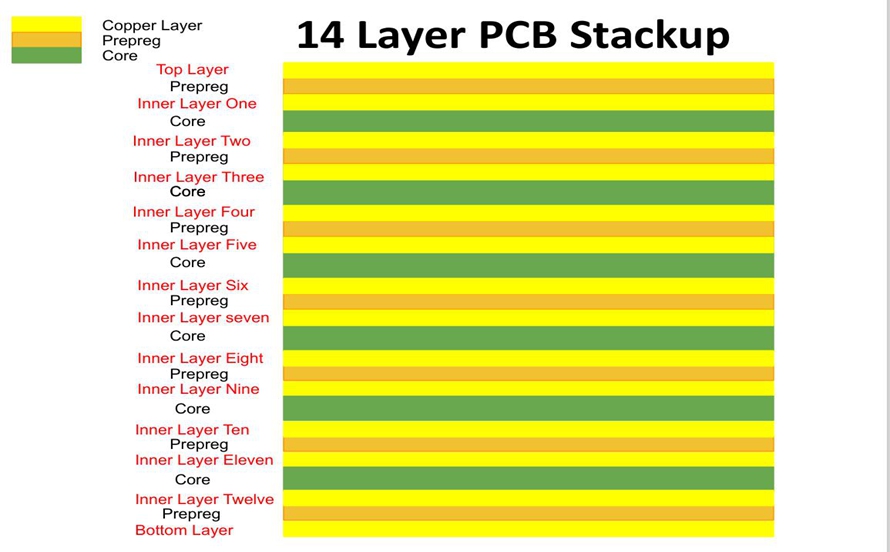
Manufacturing physics amplify these effects. Thicker foils etch slower, consuming more chemistry and increasing defect risks like over-etching in fine features. During lamination, asymmetric stackups with varying inner layer thicknesses induce warpage, as CTE mismatches between copper and dielectric exacerbate bowing. Thermal expansion during pressing cycles compounds this, potentially exceeding IPC-A-600 bow and twist limits. Engineers model these using stackup calculators to predict behavior.
Signal integrity adds another layer. While DC performance favors thicker copper for lower resistance, high-frequency signals suffer from increased dielectric losses in adjacent thicker planes. Impedance control requires consistent thickness across layers for controlled stackups. Factory insights reveal that hybrid thicknesses, thinner for signals and heavier for planes, optimize overall performance.
Material interactions influence viability. Copper foil types, such as electrodeposited or rolled annealed, exhibit varying ductility for inner layer processing. Thicker foils heighten handling risks during oxide application and black oxide treatments. Post-lamination inspection verifies thickness via cross-sectioning, confirming compliance with standards.
Manufacturing Cost Drivers Related to Inner Layer Copper Thickness
Material costs scale directly with copper weight, as heavier foils increase raw laminate expenses. Procurement of 2 oz/ft2 cores doubles the copper content compared to 1 oz/ft2, impacting PCB material selection budgets. Factories pass these premiums downstream, making cost-effective PCB design imperative for volume production.
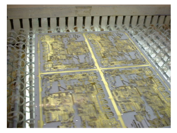
Processing costs escalate nonlinearly. Etching thicker copper prolongs cycle times, tying up equipment and raising throughput expenses. Chemical usage surges to achieve clean sidewalls, while waste disposal adds overhead. Inner layer manufacturing demands precise control to avoid shorts from incomplete etch-back, further elevating quality assurance efforts.
Lamination and drilling introduce additional burdens. Thicker inner layers resist via formation, requiring adjusted drill parameters to prevent bit wear. Sequential lamination for heavy copper extends lead times, inflating non-recurring engineering fees. Warpage mitigation, via carrier panels or constrained pressing, compounds costs for unbalanced stackups.
Yield impacts amplify expenses. Thicker copper heightens registration errors during alignment, leading to rejects. Factories report higher scrap rates for heavy inner layers in high-density boards. Optimizing to standard thicknesses minimizes these risks, supporting PCB cost optimization goals.
Performance Tradeoffs and Reliability Considerations
Thicker inner copper excels in power delivery, offering lower voltage drops and superior heat spreading for high-current planes. This suits automotive or industrial controls where reliability trumps cost. Reduced trace widths become feasible, densifying layouts without thermal runaway.
Conversely, excessive thickness degrades mechanical integrity. Boards gain weight, complicating handling and assembly. Warpage during reflow cycles intensifies, misaligning components. Signal layers benefit from thinner copper for finer lines and better impedance matching.
Reliability testing per IPC-6012 verifies these attributes. Thermal cycling exposes CTE-driven failures in thick copper laminates. Vibration tests reveal fatigue in heavy planes. Balanced selection ensures longevity across environments.
Hybrid approaches mitigate tradeoffs. Assign 1 oz/ft2 to signal inners and 2 oz/ft2 to power planes, symmetrizing the stackup. This strategy enhances performance while curbing copper thickness cost.
Best Practices for Cost-Effective Inner Layer Optimization
Start with requirements analysis. Calculate current needs using IPC-2221 charts, prioritizing thicker copper only for planes exceeding 50% area coverage. Simulate stackups for warpage, targeting symmetry within 10% thickness variance.
Collaborate early with manufacturers on capabilities. Specify nominal starting weights, accounting for 20-30% etch loss. Opt for standard foils to leverage volume pricing in PCB material selection.
Employ design rules enforcing minimum widths per thickness. Use blind vias to isolate heavy planes, reducing drill costs. Prototype iterations validate choices before production scaling.
Incorporate factory feedback loops. Post-lamination cross-sections confirm actual thicknesses. Adjust designs iteratively for yield improvements.
Document stackups rigorously, including foil types and treatments. This facilitates quoting and repeatability in inner layer manufacturing.
Conclusion
Optimizing inner layer copper thickness demands a factory-aligned approach, weighing PCB cost optimization against performance imperatives. Strategic selection of weights enhances current handling and thermal management while controlling expenses from materials and processes. Adhering to standards like IPC-6012 and IPC-2221 ensures manufacturability and reliability. Engineers achieve cost-effective PCB design by hybridizing thicknesses, symmetrizing stackups, and simulating outcomes. These practices deliver robust boards without excess spending, positioning projects for success in demanding markets.
FAQs
Q1: What factors drive copper thickness cost in inner layer manufacturing?
A1: Copper thickness cost rises with heavier foils due to increased material volume and extended etching times. Factories face higher chemical consumption and yield risks from undercutting in thick layers. Balancing with performance needs via PCB material selection keeps expenses in check. Standard weights minimize premiums while meeting specs.
Q2: How does inner layer copper thickness impact PCB performance?
A2: Thicker inner copper boosts current capacity and heat dissipation per IPC-2221 guidelines, ideal for power planes. It reduces resistance but risks warpage in asymmetric stackups. Thinner options suit signals for impedance control. Optimization ensures reliable operation across thermal cycles.
Q3: What are best practices for cost-effective PCB design with varying copper thicknesses?
A3: Prioritize thicker copper for high-current inners only, symmetrizing stackups to avoid warpage costs. Use simulations and standards for validation. Collaborate on capabilities to leverage standard foils. This approach advances PCB cost optimization without sacrificing integrity.
Q4: Why reference IPC standards for inner layer copper thickness?
A4: IPC-6012 and IPC-2221 define minimum thicknesses and design rules, ensuring process consistency. They guide current sizing and acceptability, reducing factory rejects. Compliance supports inner layer manufacturing reliability and cost predictability in multilayer boards.
References
IPC-6012E — Qualification and Performance Specification for Rigid Printed Boards. IPC, 2015
IPC-2221B — Generic Standard on Printed Board Design. IPC, 2012
IPC-A-600K — Acceptability of Printed Boards. IPC, 2020


