Introduction
Heavy copper printed circuit boards handle high current densities and demanding thermal loads in power electronics, making their fabrication a critical process for reliable performance. The heavy copper PCB manufacturing process involves specialized techniques to achieve copper thicknesses exceeding standard layers, typically starting from 3 ounces per square foot. Engineers designing for applications like power supplies, inverters, and automotive systems must understand these steps to optimize yield and functionality. Key challenges arise in heavy copper PCB etching and plating, where precision controls prevent defects like undercuts or uneven buildup. This guide outlines the heavy copper PCB fabrication workflow, drawing on factory insights to provide actionable details for electrical engineers. By following these steps, teams can produce boards that meet rigorous performance demands without compromising integrity.
What Are Heavy Copper PCBs and Why They Matter
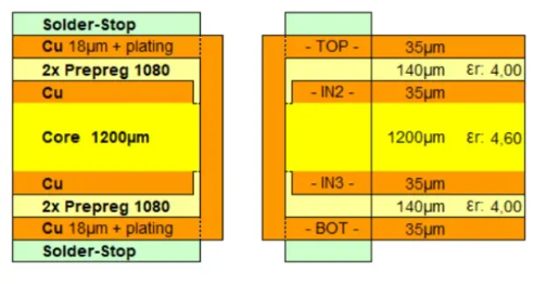
Heavy copper PCBs feature copper layers with finished weights of 3 ounces per square foot or greater, equivalent to about 105 micrometers thick, distinguishing them from standard 1-2 ounce boards. This thickness enables higher current-carrying capacity per trace width, reducing resistance and heat generation in high-power circuits. Applications span renewable energy converters, electric vehicle drivetrains, and industrial motor controls, where compact designs demand robust thermal management. Factory production scales these boards up to 20 ounces or more through additive plating, mixing heavy and standard features on the same layer for hybrid functionality. Engineers value them for minimizing layer count while enhancing mechanical strength at vias and connectors. Proper fabrication ensures compliance with performance specs, avoiding failures in thermal cycling or high-vibration environments.
The relevance intensifies in multilayer designs, where inner layers carry derated currents due to encapsulation, often limited to half the external capacity. Selecting heavy copper mitigates I-squared-R losses, supporting denser power distribution networks. From a manufacturing perspective, these boards require adjusted design rules, such as wider trace spacing and controlled aspect ratios, to accommodate plating buildup. Ultimately, they enable smaller footprints without sacrificing reliability, aligning with industry shifts toward integrated high-power modules.
Design Considerations Before Fabrication
Before initiating the heavy copper PCB manufacturing process, engineers establish design rules tailored to thick copper challenges. Minimum trace widths increase with weight, for instance, requiring at least 8 mils for 3-ounce copper at typical current loads, alongside spacing to prevent shorts post-plating. Via aspect ratios stay below 8:1 to ensure plating uniformity, with drilled holes sized larger to account for expansion. Substrate choices favor high-Tg materials above 170 degrees Celsius and low-CTE laminates under 50 ppm per degree Celsius in the z-axis for delamination resistance. Thermal relief pads incorporate spokes of 0.4 mm width and 0.25 mm gaps to balance solderability and heat transfer. These parameters guide factories in achieving plated copper thicknesses of at least 25 micrometers per IPC Class 3 requirements.
Power distribution benefits from embedded features like copper-filled vias or thermal via arrays under hotspots. Current capacity calculations per IPC-2221 help predict temperature rises, derating internal traces by 50 percent. Early collaboration with fabricators refines tolerances, as plating adds significant sidewall material affecting clearances.
The Heavy Copper PCB Manufacturing Process: Step-by-Step
1. Material Selection and Preparation
Factories begin heavy copper PCB fabrication with copper-clad laminates featuring base foils from 3 to 20 ounces, or thinner foils for subsequent buildup. High-Tg FR-4 or polyimide substrates ensure thermal stability during lamination and operation. Panels undergo cleaning and surface activation to promote adhesion in later steps. Laser direct imaging transfers patterns precisely onto thin dry films for initial etching. This preparation sets the foundation for multilayer alignment, minimizing CTE mismatches that cause warpage.
2. Inner Layer Processing and Lamination
Inner layers start with thin copper etching to define traces, followed by black oxide or alternative treatments for bond strength. Prepregs with ceramic fillers stack layers under high pressure and temperature exceeding 170 degrees Celsius. Vacuum lamination prevents voids, critical for heavy copper where thermal expansion stresses intensify. Post-lamination, X-ray verifies registration before outer processing. This step demands precise control to avoid resin flow issues with thick foils.
3. Drilling and Hole Preparation
Mechanical or laser drilling creates vias with aspect ratios under 8:1, accommodating board thicknesses up to 7 mm. Plasma or chemical desmear removes debris and resin smears from hole walls. Aspect ratio limits prevent plating voids, ensuring continuous conductivity. Factories inspect hole quality via automated systems before seeding.
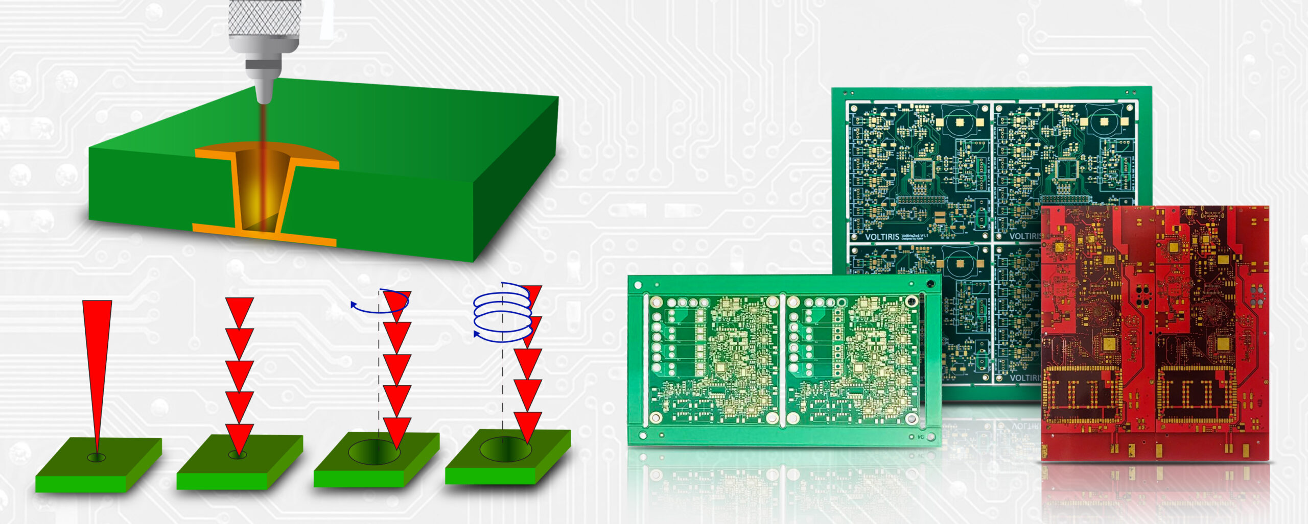
4. Electroless Plating and Heavy Copper PCB Plating
Electroless copper deposits a thin seed layer of 5 to 8 micrometers uniformly on hole walls and surfaces. Electroplating follows, using pulse techniques at 15 to 25 amps per square foot for dense buildup over 4 to 10 hours. This heavy copper PCB plating stage achieves target weights, with current density control preventing nodules or thin spots. Plated-through holes gain at least 25 micrometers sidewall copper for reliability. Factories monitor bath chemistry to sustain uniformity across large panels. The process supports mixing heavy traces with standard areas, optimizing layer efficiency.
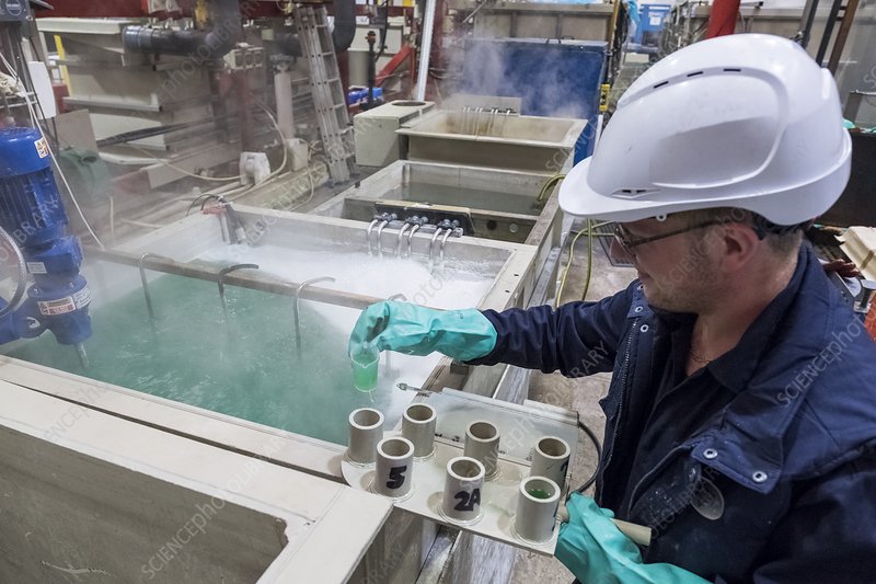
5. Pattern Transfer and Heavy Copper PCB Etching
Dry film lamination, exposure, and development define the plating pattern. Heavy copper PCB etching employs differential methods with cupric chloride and hydrochloric acid etchants at 50 degrees Celsius, targeting an etch factor above 3:1. This produces straight sidewalls, minimizing undercuts that plague isotropic etching of thick copper. Temperature and conveyor speed control ensure consistent lateral etch rates. Post-etch stripping and cleaning prepare surfaces for imaging. Factories use high-speed or step etching to handle 20-ounce features without trapezoidal profiles.
6. Outer Layer Finishing and Mechanical Processing
Solder mask application uses thicker liquid photoimageable films to cover heavy traces adequately. Silkscreen adds legends, followed by surface finishes like ENIG or HASL for protection. Routing, scoring, and beveling shape panels, with tabs for handling. Countersinking addresses connector pins in thick boards.
7. Inspection and Testing
Automated optical inspection detects defects post-etching. Flying probe electrical testing verifies continuity and shorts. X-ray measures copper thickness, while warpage checks ensure planarity. Thermal cycling from -55 to 150 degrees Celsius simulates service conditions. IPC-6012 qualification specs guide final acceptance, confirming performance for rigid boards.
Challenges in Heavy Copper PCB Manufacturing and Best Practices
Differential etching demands precise chemistry to counter slow vertical versus lateral rates in thick copper, avoiding over-etching that narrows traces. Plating uniformity falters without pulse reversal, leading to dog-boning in vias. Warpage from asymmetric copper distribution requires balanced layouts and constrained fixturing during lamination. Best practices include starting with thin base foils for plating buildup, enabling finer features than direct thick etching. IPC-A-600 acceptability criteria evaluate conductor edges and plating coverage post-fabrication. Factories mitigate delamination via low-CTE prepregs and controlled cure cycles.
For vias, epoxy filling enhances thermal paths while plating reinforces walls. Design per IPC-2221 current charts prevents hotspots, with external traces outsizing internals. Ionography testing confirms cleanliness before shipping.
Conclusion
Mastering the heavy copper PCB manufacturing process unlocks robust solutions for high-power electronics, from plating buildup to precise etching. Engineers benefit from understanding these factory-driven steps to refine designs early. Adhering to standards ensures quality, minimizing rework in production. This approach delivers boards with superior current handling and thermal resilience.
FAQs
Q1: What is the heavy copper PCB manufacturing process?
A1: The heavy copper PCB manufacturing process starts with material preparation using thick-clad laminates, proceeds through drilling, electroless seeding, and extended electroplating for copper buildup. Lamination aligns multilayers, followed by differential etching for trace definition. Final steps include solder mask, finishing, and rigorous testing like AOI and thermal cycling. This workflow handles thicknesses from 3 to 20 ounces, prioritizing uniformity and minimal defects for high-reliability applications.
Q2: How does heavy copper PCB etching differ from standard processes?
A2: Heavy copper PCB etching uses differential techniques with controlled etchants like cupric chloride at specific temperatures to achieve high etch factors above 3:1. This counters undercuts in thick layers, producing straighter sidewalls than isotropic methods on thin copper. Factories adjust conveyor speeds and chemistry for precision, inspecting via AOI for edge quality. It demands specialized equipment to maintain trace integrity without trapezoidal profiles.
Q3: What are key steps in heavy copper PCB plating?
A4: Heavy copper PCB plating begins with electroless seed deposition, followed by pulse electroplating at optimized current densities of 15 to 25 amps per square foot. This builds uniform thicknesses over hours, supporting via filling and trace enhancement. Bath monitoring prevents defects like nodules, ensuring at least 25 micrometers on walls. The process enables hybrid boards with mixed copper weights for efficient power distribution.
Q4: Why is quality control vital in heavy copper PCB fabrication?
A4: Quality control in heavy copper PCB fabrication verifies plating uniformity, etch profiles, and warpage via X-ray, AOI, and electrical tests. It aligns with IPC standards for conductor thickness and adhesion, preventing field failures from thermal stress. Factories conduct thermal cycling to simulate loads, confirming via reliability. This step ensures boards meet performance specs in demanding environments like power electronics.
References
IPC-6012E — Qualification and Performance Specification for Rigid Printed Boards. IPC, 2017
IPC-A-600K — Acceptability of Printed Boards. IPC, 2020
IPC-2221B — Generic Standard on Printed Board Design. IPC, 2012


