Introduction
Electrical engineers face increasing demands for compact PCBs with high interconnect density in applications ranging from telecommunications to computing systems. Blind vias connect an outer layer to one or more inner layers without penetrating the full board thickness, while buried vias link only inner layers, remaining invisible on the surfaces. These structures optimize routing space, shorten signal paths to minimize inductance and capacitance, and enhance overall signal integrity compared to traditional through-hole vias. Sequential lamination emerges as the cornerstone manufacturing method, allowing precise formation of these vias through multiple controlled build-up cycles. By mastering the blind via manufacturing process, buried via design guidelines, and sequential lamination via formation, engineers can achieve reliable advanced interconnects. This article delivers factory-driven insights into their implementation, drawing on established processes to support robust PCB designs.
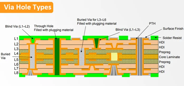
What Are Blind and Buried Vias and Why Do They Matter?
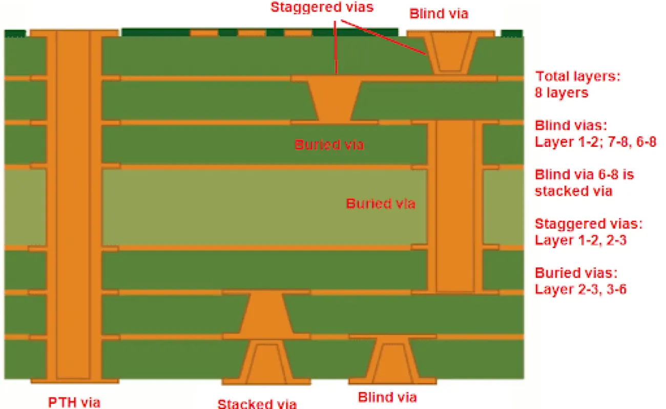
Blind vias start from an external layer and terminate at a specific inner layer, freeing surface pads for components and enabling denser layouts. Buried vias interconnect multiple inner layers exclusively, maximizing inner layer routing efficiency without surface exposure. Together, they reduce via stub lengths, which lowers parasitic effects critical for high-speed signals in multilayer boards. In complex designs, these vias support finer pitch components and more layers within the same footprint, addressing the challenges of miniaturization. Their relevance grows in high-density interconnect boards where through vias would consume valuable real estate and degrade performance. Factory experience shows that proper use of blind and buried vias can significantly improve yield when aligned with manufacturing capabilities.
These vias matter because they enable shorter electrical paths, reducing signal loss and crosstalk in demanding electrical environments. Engineers benefit from increased layer count flexibility, allowing more power and ground planes for better thermal management. However, their implementation requires careful planning to avoid fabrication pitfalls like misalignment. Overall, blind and buried vias represent a shift toward efficient, performance-oriented PCB architectures essential for modern electronics.
Technical Principles of Sequential Lamination Via Formation
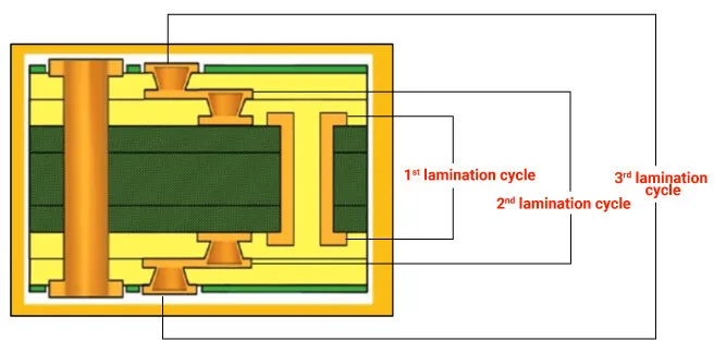
Sequential lamination via formation builds PCBs iteratively by creating sub-stacks or subsets of layers, drilling and plating vias within them, then bonding via additional prepreg sheets. This differs from single-cycle lamination by allowing targeted via structures that span specific layer pairs, essential for blind and buried vias. The process begins with processing inner layer cores, such as etching signal patterns on copper-clad laminates for layers two and three. Prepreg sheets and outer copper foils are then aligned and laminated to form the first subset, followed by drilling for blind vias that connect, for example, layers one through four.
After drilling, the subsets undergo imaging, electroplating to fill vias with copper, and etching to define circuits, with one side often serving as a panel plate for uniform plating. Multiple subsets are prepared similarly, ensuring vias like buried connections between layers five and six are formed in their respective stacks. These subsets are then sequentially laminated together using prepreg for adhesion, with alignment pins maintaining registration across cycles. High-pressure, heated presses cure the resin, bonding layers permanently while filling vias for structural integrity. This sequential approach achieves consistent aspect ratios across drills, a key advantage for reliable plating in blind via manufacturing process.
The blind via manufacturing process integrates mechanical or laser drilling post-subset lamination but pre-final assembly, controlling depth to target inner layers precisely. Buried vias form analogously within inner subsets, avoiding outer exposure. Each cycle introduces potential shrinkage, managed through scaling techniques to preserve layer-to-layer alignment. Factory protocols emphasize cleaning residues after each press to prevent defects, culminating in final through-hole processing if needed.
Buried Via Design Guidelines and Practical Best Practices
Buried via design guidelines emphasize non-overlapping spans to simplify sequential lamination, such as avoiding a buried via from layers two to four alongside a blind via from one to three. Engineers should define stack-ups clearly in design data, specifying via starts and ends to guide subset construction. IPC-2221 provides foundational rules for via sizing, annular rings, and layout to ensure manufacturability. Nesting spans rather than crossing them reduces plating complexity and maintains uniform copper deposition. Collaboration with fabricators early optimizes prepreg selection for flow into vias, promoting capped structures for enhanced reliability.
Practical best practices include verifying aspect ratios suitable for drilling methods, with mechanical vias favoring balanced depths per layer. Use alignment aids like pins during lamination to counteract registration shifts from thermal expansion. Post-lamination copper reduction on thicker outer layers improves etching yield and impedance control. IPC-6012 outlines qualification criteria for via performance in rigid boards, stressing plating thickness and adhesion. These steps mitigate common issues, ensuring buried vias support high-density routing without compromising signal paths.
For blind vias, similar guidelines apply, prioritizing controlled-depth drilling in subsets to prevent breakthroughs. Factory insights recommend two prepreg layers in final bonds for better resin flow and via filling. Overall, adhering to these practices balances density gains with fabrication feasibility.
- Blind — Connection: Outer to Inner; Key Design Consideration: Depth control in subsets
- Buried — Connection: Inner to Inner; Key Design Consideration: Non-overlapping spans
Challenges in Sequential Lamination and Mitigation Strategies
Sequential lamination introduces challenges like warpage from asymmetric copper weights across sub-stacks, as multiple plating cycles thicken certain layers. Mitigation involves symmetric build-ups where possible and controlled cooling post-press to stabilize dimensions. Registration errors from shrinkage demand precise pin alignment and data scaling in design files. Cost escalates with each lamination cycle due to added handling and yield risks, so minimizing cycles through efficient via planning is crucial.
Via plating uniformity poses risks, addressed by electroplating protocols ensuring adequate copper buildup per IPC-4761 via protection guidelines. Overlapping via configurations amplify these issues, leading to lower yields, so design reviews focus on staggered structures. Factory-driven testing, including cross-section analysis, verifies integrity before full production.
Conclusion
Mastering blind and buried vias through sequential lamination unlocks advanced interconnects for high-performance PCBs. The blind via manufacturing process and sequential lamination via formation enable precise layer-specific connections, while buried via design guidelines ensure reliable implementation. By understanding technical principles, applying best practices, and addressing challenges like warpage and alignment, electrical engineers can achieve denser, faster boards. Factory-aligned designs adhering to standards like IPC-2221 and IPC-6012 deliver consistent results. Embracing these techniques positions designs for success in demanding applications.
FAQs
Q1: What is the blind via manufacturing process using sequential lamination?
A1: The blind via manufacturing process involves building layer subsets, laminating cores with prepregs and foils, then drilling controlled-depth holes before plating and etching. Subsets are sequentially bonded, with alignment pins ensuring registration. This iterative approach forms vias from outer to inner layers without full penetration, maintaining consistent aspect ratios. Factories optimize cycles to balance complexity and yield.
Q2: What are key buried via design guidelines for multilayer PCBs?
A2: Buried via design guidelines recommend non-overlapping spans, nested configurations, and clear stack-up definitions to simplify sequential lamination. Follow IPC-2221 for annular ring and sizing rules to support plating reliability. Avoid crossing with blind vias to reduce fabrication risks. Early fabricator input refines prepreg flow for capped structures. These practices enhance inner layer routing density.
Q3: How does sequential lamination via formation differ from standard lamination?
A3: Sequential lamination via formation uses multiple cycles to build and bond subsets, enabling blind and buried vias through targeted drilling and plating. Standard lamination processes all layers at once, limiting via types to through-holes. This method supports complex HDI structures but requires alignment controls against shrinkage. It achieves shorter vias for better signal integrity.
Q4: What challenges arise in sequential lamination for advanced vias?
A4: Challenges include warpage from uneven copper plating, registration shifts, and higher costs per cycle. Mitigation uses symmetric stacks, scaling data, and precise alignment. IPC-6012 qualification verifies via performance. Optimizing via spans minimizes issues while maximizing density benefits. Factory protocols ensure robust outcomes.
References
IPC-2221B — Generic Standard on Printed Board Design. IPC, 2012
IPC-6012DS — Qualification and Performance Specification for Rigid Printed Boards. IPC, 2015
IPC-4761 — Via Protection, Filled and Covered for Printed Boards. IPC, 2020