Introduction
Double-sided PCB assembly represents a cornerstone in modern electronics manufacturing, enabling higher component density and functionality in compact devices. Engineers often encounter challenges when components populate both sides of the board, requiring precise coordination between surface-mount technology (SMT) and through-hole technology (THT). Mastering double-sided PCB assembly ensures reliable performance, minimizes defects, and optimizes production yields. This article delves into essential PCB soldering techniques, SMT assembly processes, through-hole assembly methods, and PCB assembly best practices tailored for electrical engineers. By understanding these elements, teams can troubleshoot issues proactively and achieve consistent quality. Key to success lies in adhering to established processes that balance speed, precision, and reliability.
What Is Double-Sided PCB Assembly and Why It Matters
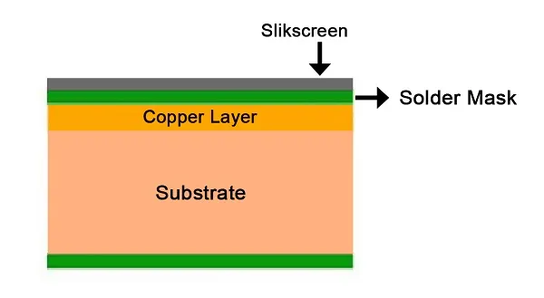
Double-sided PCB assembly involves placing and soldering electronic components on both the top and bottom surfaces of a printed circuit board. This approach contrasts with single-sided boards by allowing greater circuit complexity within the same footprint, making it ideal for applications like consumer electronics, automotive controls, and industrial sensors. SMT assembly dominates on one side for fine-pitch parts, while through-hole assembly secures larger components that penetrate the board. The process demands careful sequencing to avoid interference between layers during soldering. Industry relevance stems from its cost-effectiveness and versatility, as double-sided boards support mixed-technology designs without escalating to multilayer stacks.
Engineers value double-sided PCB assembly for its ability to handle power and signal integrity demands in space-constrained environments. Reliability hinges on preventing issues like component shadowing or thermal mismatches during reflow. As device miniaturization accelerates, proficiency in these techniques directly impacts prototyping success and high-volume production. PCB assembly best practices here reduce rework cycles and enhance overall yield rates. For electrical engineers, grasping these fundamentals translates to fewer field failures and smoother design iterations.
Technical Principles of Double-Sided PCB Assembly
The foundation of double-sided PCB assembly rests on the interplay between SMT and through-hole components, each with distinct attachment mechanisms. SMT parts adhere via solder paste applied through stencils, enabling automated placement and reflow soldering. Through-hole components feature leads that insert into plated vias, relying on wave soldering or manual methods for fixation. In double-sided designs, the top side typically hosts primary SMT populations, while the bottom accommodates THT or secondary SMT after initial processing. Thermal management proves critical, as uneven heating can cause warpage or delamination.
PCB soldering techniques vary by component type and board configuration. Reflow soldering suits SMT assembly, where controlled oven profiles melt paste into joints following predefined ramp-soak-peak cycles. Wave soldering excels for through-hole assembly, immersing the board underside in molten solder while flux activates surfaces. Selective soldering emerges for mixed boards, targeting specific THT leads without disturbing adjacent SMT joints. Adherence to J-STD-001 standards ensures joint integrity, specifying criteria for fillet formation and hole fill.
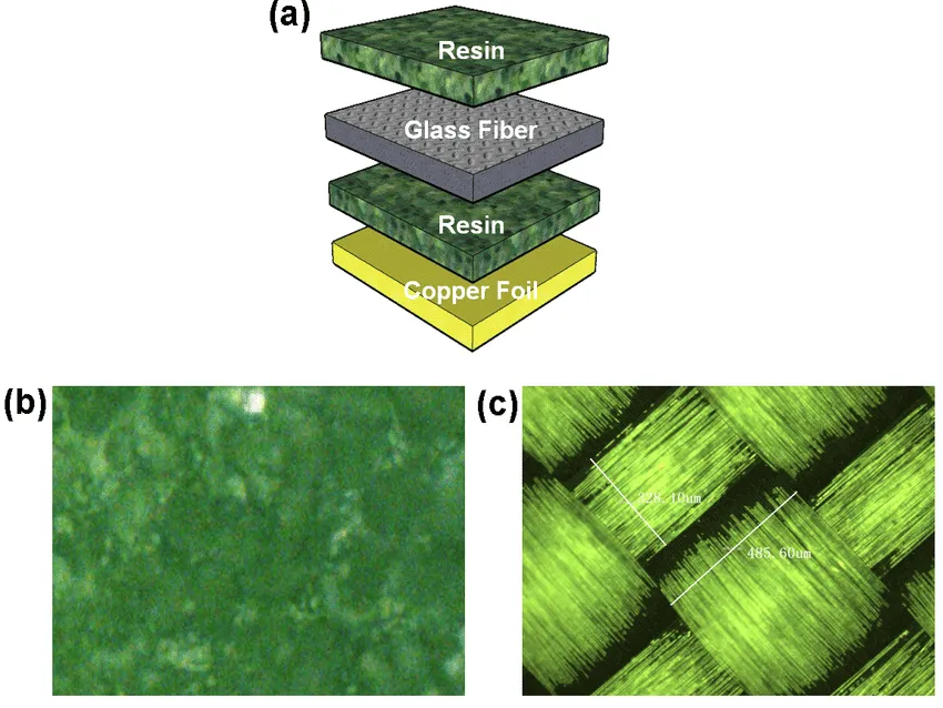
Material interactions influence assembly outcomes significantly. Solder paste composition, including alloy type and flux activity, must match board finishes like HASL, ENIG, or OSP to prevent defects. Component lead coplanarity tolerances affect placement accuracy, particularly for fine-pitch QFPs or BGAs on the top side. Board warpage from CTE mismatches between copper and substrate exacerbates bottom-side challenges during wave soldering. Engineers mitigate these by selecting low-stress laminates and validating profiles empirically.
Inspection principles underpin quality at each stage. Automated optical inspection (AOI) verifies post-print paste volume and placement offsets before reflow. X-ray imaging reveals hidden through-hole fill and BGA voids non-destructively. Electrical testing confirms continuity across both sides post-assembly. These methods align with IPC-A-610 acceptability classes, distinguishing cosmetic from functional defects.
PCB Assembly Best Practices for Double-Sided Boards
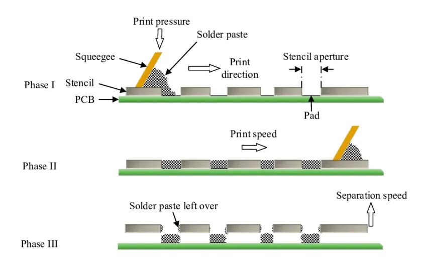
Effective double-sided PCB assembly begins with meticulous preparation to sequence operations logically. Start by populating the side with more sensitive or denser SMT components first, typically the top, to shield them from subsequent handling. Apply solder paste uniformly using laser-cut stencils with 5-10% wall thickness relative to aperture size for clean release. Verify paste height with SPI systems targeting 75-125% volume over pads. Placement machines should achieve ±25μm accuracy for 0201 parts, minimizing offsets that lead to bridging.
Reflow soldering demands optimized profiles tailored to the assembly. Preheat gradually to 150°C over 60-120 seconds to activate flux without spattering, followed by a soak at 180°C for alloy homogenization. Peak temperatures hover at 245-260°C for SAC305 paste, holding 30-60 seconds above liquidus. Cooling rates below 6°C/second prevent thermal shock to bottom-side prep. Monitor with thermocouples at multiple zones, adjusting conveyor speed for nitrogen atmospheres to reduce oxidation.
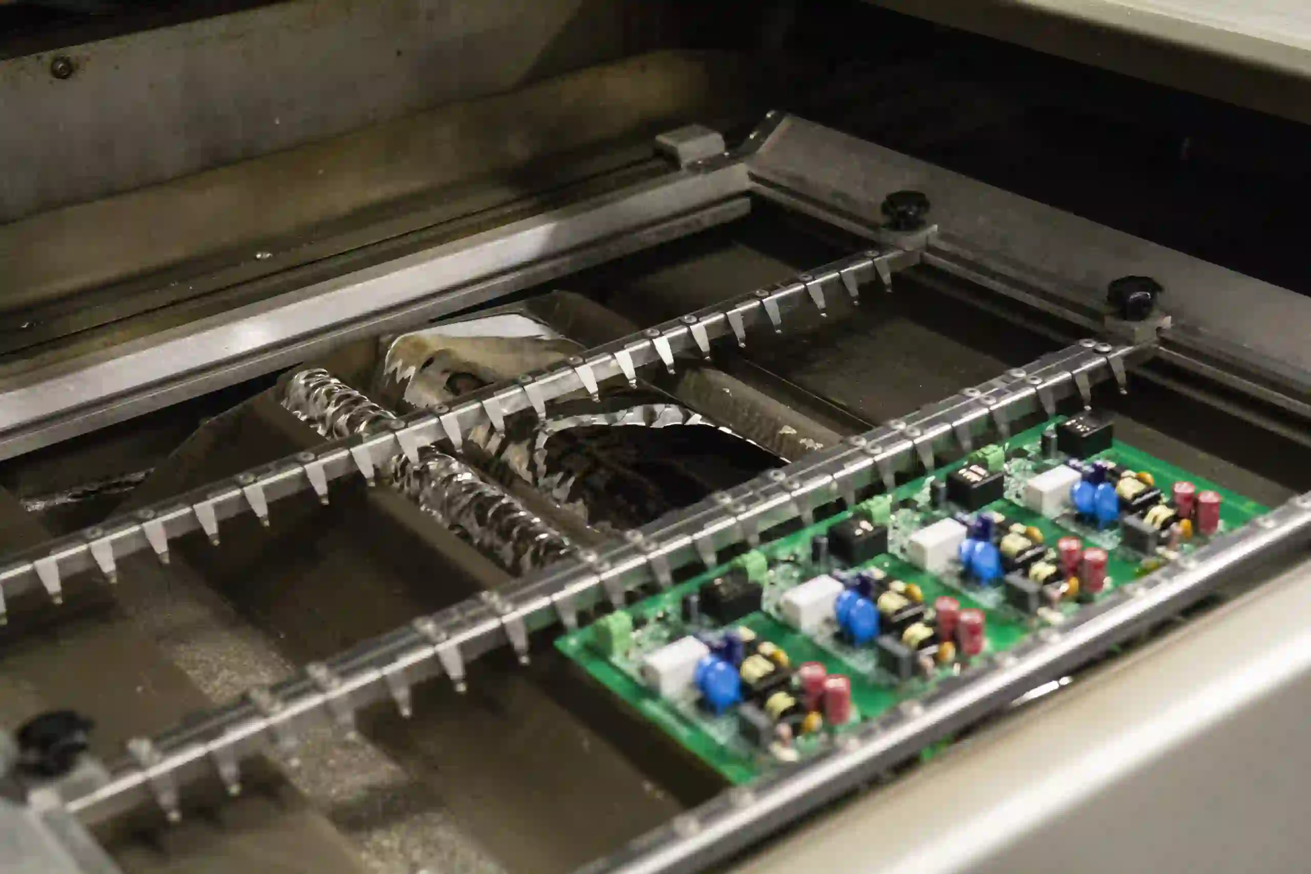
For through-hole assembly on the bottom side, wave soldering follows SMT reflow with masking to protect top components. Flux application ensures clean barrel walls, aiming for 75-100% hole fill per J-STD-001. Preheat the board to 100-120°C to minimize thermal gradients. Solder pot temperatures stabilize at 250-260°C, with laminar flow impingers for smooth wetting. Post-wave cleaning removes residues using DI water or saponifiers, followed by drying to prevent dendritic growth.
PCB soldering techniques extend to rework scenarios, where IPC-7711/7721 guidelines dictate hot air or conduction tools for removal. Preserve adjacent joints by localized heating below 350°C, using flux to aid wetting. For double-sided boards, secure the opposite side with fixtures to counter flexing. Post-rework, reinspection via AOI or cross-sectioning validates integrity.
Advanced best practices incorporate design for assembly (DFA) rules early. Specify fiducials on both sides for machine alignment, with at least three per panel. Panelize boards with v-scoring for stability during transport. Implement 100% inline AOI post-placement and post-reflow, flagging opens, shorts, or polarity errors. Functional testing under power-up sequences detects latent issues like via cracks from board flex.
Yield tracking refines processes iteratively. Log defect Pareto charts to prioritize root causes, such as tombstoning from rapid cooling or bridging from excess paste. Statistical process control monitors Cpk values above 1.33 for critical parameters. Collaborate across design, fabrication, and assembly to refine land patterns per IPC-7351.
Common Troubleshooting Challenges in Double-Sided PCB Assembly
Tombstoning plagues SMT assembly when surface tension imbalances lift chip ends during reflow. Causes include pad imbalance, excessive preheat ramps, or moisture-laden components. Mitigate by equalizing pad sizes, slowing ramp rates to 1-2°C/second, and baking parts per JEDEC J-STD-033. Verify with thermal profiling to ensure symmetric melting.
Solder bridging connects adjacent pads, often from paste smearing or high reflow peaks. Stencil snap-off optimization and reduced squeegee pressure help, alongside lower-volume printing. For bottom-side SMT, glue dots secure parts pre-reflow against gravity-induced shifts.
Through-hole voids arise from flux exhaustion or solder starvation. Extend preheat for flux volatilization and ensure drag-out rates support wetting. X-ray confirms fill percentages, triggering process tweaks.
Warpage distorts double-sided boards during wave soldering, cracking top-side joints. Thinner cores and symmetric copper pours counteract this. Fixturing pallets flatten boards in the wave machine.
Conclusion
Mastering double-sided PCB assembly hinges on integrating SMT assembly, through-hole assembly, and precise PCB soldering techniques with rigorous PCB assembly best practices. Engineers achieve superior yields by sequencing operations thoughtfully, optimizing thermal profiles, and leveraging inline inspections. Standards like IPC-A-610, J-STD-001, and IPC-7711/7721 provide the benchmark for acceptability and rework. Troubleshooting empowers proactive defect prevention, ensuring robust electronics. Prioritizing these elements elevates design reliability and production efficiency across applications.
FAQs
Q1: What are the key differences between SMT assembly and through-hole assembly in double-sided PCB assembly?
A1: SMT assembly places components directly on surface pads using solder paste and reflow, ideal for high-density top-side populations. Through-hole assembly inserts leads into vias for wave or selective soldering, suiting robust bottom-side connections. Double-sided boards sequence SMT first to protect it from THT flux and heat. Best practices include masking and fixturing to prevent interactions. This mixed approach maximizes functionality while adhering to J-STD-001 joint criteria.
Q2: How do PCB soldering techniques impact double-sided PCB assembly quality?
A2: Reflow soldering ensures uniform SMT joints via controlled profiles, while wave soldering fills through-hole vias efficiently. Selective soldering targets hybrids without disturbing prior work. Poor profiles cause defects like voids or bridging, addressed by thermocouple validation. Flux selection matches finishes for wetting. Consistent techniques per IPC-A-610 boost reliability in double-sided designs.
Q3: What are essential PCB assembly best practices for avoiding defects in double-sided boards?
A3: Prioritize top-side SMT placement before bottom THT to minimize handling damage. Optimize stencil printing for paste volume and use AOI at each stage. Thermal profiling prevents warpage during reflow and wave steps. Bake components to eliminate moisture. Track yields with Pareto analysis for continuous improvement.
Q4: Why is inspection critical in double-sided PCB assembly processes?
A4: Inspection verifies paste deposition, placement accuracy, and joint formation across both sides. AOI catches pre-reflow errors, X-ray detects hidden voids in vias. Electrical testing confirms functionality post-assembly. This multilayered approach aligns with standards, reducing escapes and rework costs.
References
IPC-A-610H — Acceptability of Electronic Assemblies. IPC, 2019
J-STD-001G — Requirements for Soldered Electrical and Electronic Assemblies. IPC, 2011
IPC-7711/7721B — Rework, Modification and Repair of Electronic Assemblies. IPC, 2018