Why is PCB impedance simulation vital for signal integrity?
Impedance control is a foundational element in contemporary printed circuit board (PCB) design, particularly critical for high-speed circuits where maintaining signal integrity is paramount for reliable performance. Inconsistent or mismatched impedance can lead to severe signal degradation phenomena, including reflections, crosstalk, and timing inaccuracies. These issues can culminate in data corruption, intermittent system failures, or complete operational shutdowns. For electrical engineers developing designs that operate at frequencies exceeding 100 MHz, the practice of simulating impedance is no longer merely advantageous; it has become an absolute necessity to prevent such costly complications.
This discussion aims to thoroughly explore the domain of PCB impedance simulation, delving into the specialized software tools engineered for precise analysis, and outlining proven techniques to verify impedance control. Whether your focus is on telecommunications, automotive electronics, or sophisticated consumer devices, the insights provided here will empower you to achieve highly reliable and efficient designs. Understanding the fundamental reasons why impedance is crucial and how simulation facilitates its management is the essential starting point.

The critical role of impedance in high-speed PCB performance
Impedance, within the context of a PCB, refers to the effective opposition a circuit presents to the flow of alternating current (AC). This characteristic is influenced by several physical design parameters, including the width of conductive traces, the dielectric properties of the insulating material, and the overall layer stack-up configuration. For high-speed signals, maintaining a consistent and controlled impedance—typically 50 ohms for single-ended signals or 75 ohms for video, or 100 ohms for differential pairs—is crucial. This consistency ensures that signals propagate along the traces without significant reflection back towards the source or excessive signal loss, which would otherwise degrade the signal's quality.
Even a relatively small impedance mismatch, potentially as low as 10%, can introduce reflections that significantly compromise signal integrity, leading to data errors and functional instability. PCB impedance simulation empowers engineers to accurately predict and analyze signal behavior before the manufacturing phase. By identifying potential issues such as unwanted crosstalk or critical signal delays during the design stage, engineers can proactively implement corrective measures, thereby avoiding the substantial time and financial PCB cost associated with design revisions or the failure of physical prototypes. For example, in a advanced 5G communication board operating at 3.5 GHz, even a minor deviation from the target impedance can result in considerable signal degradation, underscoring simulation as an indispensable step in the design workflow.
What are the leading software tools for PCB impedance simulation?
Selecting the appropriate PCB impedance simulation software is a critical decision that directly impacts the accuracy and reliability of your high-speed circuit designs. Modern electronic design automation (EDA) suites offer robust capabilities for simulating signal integrity.
Top software options for precise impedance analysis
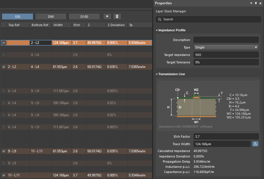
Altium Designer is a widely adopted EDA tool known for its integrated impedance calculation and comprehensive signal integrity analysis features. Its xSignal feature, for instance, enables detailed analysis of high-speed designs, including precise impedance control for both differential pairs and single-ended traces. Altium's simulation capabilities facilitate the definition of intricate stack-up configurations and trace geometries to achieve target impedance values, typically within a tight tolerance of ±5%. A practical application involves using Altium’s layer stack manager to input specific dielectric constants and trace dimensions for a desired 50-ohm controlled impedance line, followed by executing a signal integrity check to verify performance at frequencies extending up to 10 GHz.
Cadence Allegro PCB Designer provides an advanced suite of simulation functionalities through its integrated Signal Integrity (SI) tools. This platform supports both pre-layout planning and post-layout verification, allowing engineers to simulate impedance and detect potential issues such as crosstalk or jitter with high fidelity. Cadence further enhances its capabilities through integration with Sigrity, a specialized tool suite for comprehensive power and signal integrity analysis, making it an ideal choice for highly complex, multi-layer board designs. For example, in a DDR4 memory interface operating at 3200 MT/s, Cadence can accurately simulate impedance across multiple layers to ensure critical timing margins are met, thereby significantly reducing the likelihood of data errors.
ANSYS SIwave stands out as a powerful electromagnetic simulation tool specifically focused on signal and power integrity. It excels in modeling impedance for high frequency PCB designs and provides detailed 3D electromagnetic field analysis. SIwave is particularly valuable for engineers working on RF or microwave circuits where extremely precise impedance matching (e.g., 50 ohms for RF transmission lines) is absolutely critical. In a practical use case, for a 24 GHz radar PCB, SIwave can simulate the impedance of microstrip lines and effectively identify subtle parasitic effects that might otherwise degrade signal quality.
HyperLynx by Mentor Graphics offers robust signal integrity simulation capabilities, including comprehensive impedance analysis tailored for high-speed digital designs. It features user-friendly wizards that expedite the setup of impedance-controlled traces and supports batch simulations, enabling engineers to analyze multiple design scenarios efficiently. HyperLynx is renowned for its intuitive interface, making it accessible even for engineers who are relatively new to signal integrity simulation. A practical application involves using HyperLynx to simulate a 100-ohm differential pair for a USB 3.0 design, allowing for iterative adjustments to trace spacing and width to achieve the target impedance within a tight ±3% tolerance
What are effective techniques for simulating signal integrity?
Beyond selecting robust PCB design software, the application of effective simulation techniques is paramount for accurately verifying impedance control and ensuring reliability in PCB designs. These proven methods help engineers systematically address potential signal integrity issues.
Methodologies for accurate impedance control verification
Pre-layout simulation involves performing impedance analysis before the finalization of the physical PCB layout. This early-stage analysis allows engineers to define the layer stack-up, trace widths, and spacing, thereby predicting impedance values and adjusting initial design parameters proactively. For instance, to achieve a 50-ohm impedance for a microstrip trace on a standard FR-4 substrate (with a dielectric constant of approximately 4.2), a pre-layout simulation might determine an optimal trace width of 7 mils. The steps typically include defining the target impedance based on the application (e.g., 50 ohms for RF, 100 ohms for differential pairs), modeling the stack-up and trace geometry using simulation software, and iteratively adjusting parameters like trace width or dielectric thickness until the target impedance is met.
Following the completion of the physical layout, post-layout verification is crucial. This step involves simulating the actual design to confirm that it maintains the intended impedance characteristics, accounting for real-world factors such as manufacturing tolerances and parasitic effects introduced by vias or component pads. Tools like Cadence Allegro or HyperLynx can extract the detailed layout geometry and simulate impedance across all critical nets. For example, in a 10-layer PCB designed for a server application, a post-layout simulation might reveal that a specific trace routed near a power plane exhibits an impedance of 53 ohms, slightly deviating from the target 50 ohms, prompting a localized redesign of trace spacing.
For high-speed designs, differential pair impedance control is essential. Differential pairs, commonly used in interfaces like USB, HDMI, or Ethernet, require precise impedance matching, typically 90 or 100 ohms. Simulation tools are critical for accurately modeling the electromagnetic coupling between the two traces to ensure consistent differential impedance. A common challenge is uneven spacing between the traces, which can lead to an impedance mismatch of up to 10 ohms, resulting in detrimental signal skew. Designers should use simulation software to test various trace separations and edge-coupling configurations to achieve the desired differential impedance within a tight tolerance, usually ±5%.
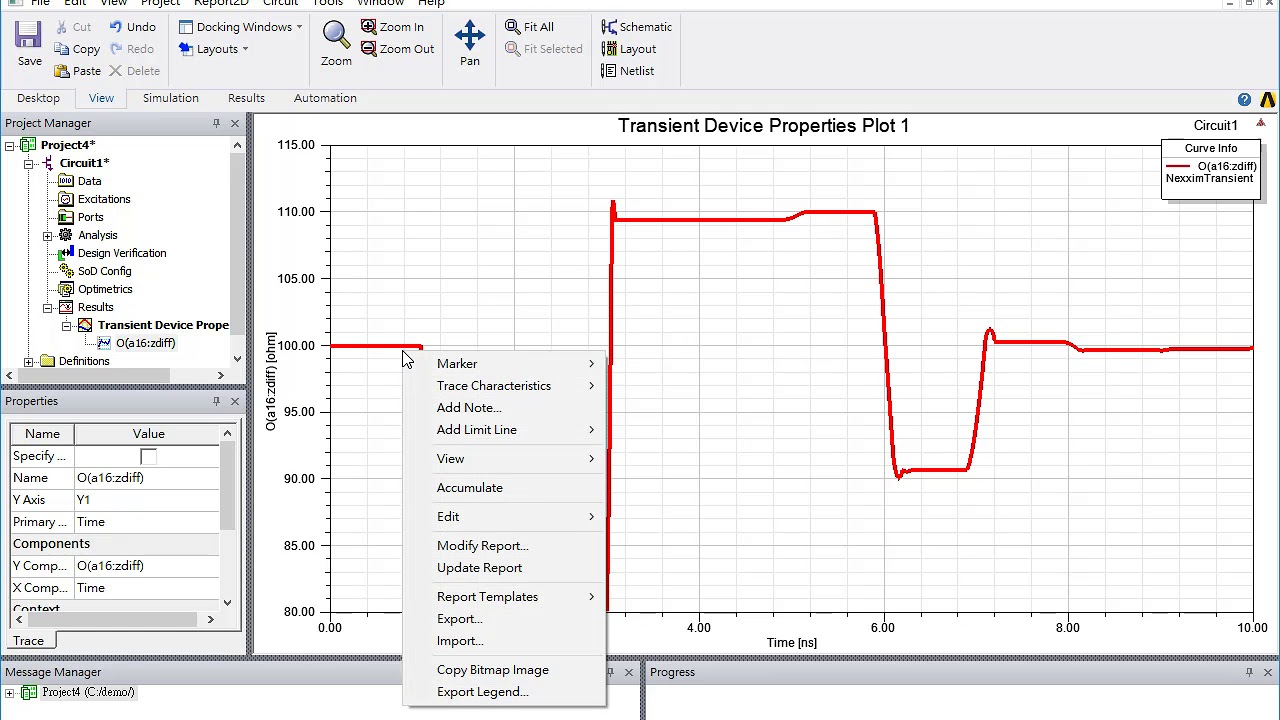
Finally, Time-Domain Reflectometry (TDR) simulation is an advanced technique used to identify impedance discontinuities along a transmission line. By simulating the injection of a fast electrical pulse and analyzing the characteristics of the reflected signal, engineers can pinpoint exact locations and magnitudes of impedance mismatches or abrupt changes. Many modern simulation tools, such as ANSYS SIwave, integrate TDR analysis to provide a visual representation of impedance variations along a trace. For a PCIe Gen 4 design operating at 16 GT/s, TDR simulation can detect a sudden impedance change at a via transition, allowing engineers to implement corrective actions such as adding stitching vias or adjusting the via geometry for a smoother signal flow.
What challenges arise in PCB impedance simulation?
While PCB impedance simulation is an invaluable tool, engineers often encounter several challenges that can impact the accuracy and reliability of their results. Addressing these complexities is crucial for successful high-speed design.
Overcoming material, manufacturing, and high-frequency complexities
One significant challenge stems from material variability. The dielectric constant (Dk) of common PCB materials like FR-4 can fluctuate (typically between 4.0 and 4.5), which directly affects impedance calculations. To mitigate this, engineers should always use precise dielectric property data provided by the PCB manufacturer and perform simulations across a range of possible Dk values to account for inherent material tolerances.
Manufacturing tolerances present another hurdle. Inaccuracies during the etching process or slight misalignments of layers can alter trace dimensions and spacing, consequently affecting the actual impedance. Close collaboration with the PCB fabricator is essential to understand their specific manufacturing capabilities and tolerances (e.g., ±10% variation on trace width) and incorporate these into the simulation models.
Furthermore, at higher frequencies, typically above 1 GHz, high-frequency effects become increasingly significant. Phenomena such as the skin effect, where current flows predominantly on the surface of conductors, and dielectric loss, where energy is absorbed by the insulating material, can alter the effective impedance of traces. It is imperative to use simulation tools that are capable of accounting for frequency-dependent behavior and, whenever possible, validate simulation results with real-world physical testing to ensure accuracy in these high-frequency regimes.
Best practices for verifying impedance control in PCB design
To maximize the effectiveness of PCB impedance simulations and consistently achieve successful high-speed designs, engineers should integrate several best practices into their design and verification workflows. These strategies promote accuracy, efficiency, and collaboration.
Strategies for robust impedance-controlled designs
Collaborate early and often with your PCB manufacturer. Engage with them during the initial design phases to confirm the precise material properties (like dielectric constant and loss tangent) and their specific fabrication capabilities, including minimum trace widths, spacing, and stack-up options. This early collaboration can prevent costly redesigns later in the project.
Iterate and validate your designs rigorously. Do not rely on a single simulation run. Instead, perform multiple simulations by varying key parameters within their expected tolerance ranges. This helps identify the most robust design that performs reliably even under minor manufacturing variations. Once prototypes are available, validate your simulation results through physical measurements using instruments like Time-Domain Reflectometers (TDRs).
Document results comprehensively. Maintain detailed records of all simulation settings, input parameters, and results. This documentation is invaluable for future projects, for troubleshooting unforeseen issues, and for demonstrating compliance with design specifications.
Finally, stay updated with the latest advancements in PCB impedance simulation software. EDA tools are constantly evolving, offering improved algorithms, enhanced features for signal integrity analysis, and more accurate material models. Utilizing the latest versions ensures you have access to the most advanced capabilities for tackling complex high-speed design challenges.
Mastering PCB impedance simulation for superior designs
PCB impedance simulation has emerged as an indispensable component of modern PCB design, particularly crucial for high-speed applications where maintaining pristine signal integrity is paramount. By effectively leveraging powerful PCB impedance simulation software—such as Altium Designer, Cadence Allegro, ANSYS SIwave, and HyperLynx—and by systematically applying advanced techniques like pre-layout analysis, comprehensive post-layout verification, and detailed Time-Domain Reflectometry (TDR) simulation, electrical engineers can achieve precise impedance control and ensure robust, reliable performance.
For engineers, mastering these specialized tools and techniques translates directly into significant advantages: fewer design iterations, reduced overall costs, and accelerated time-to-market for their products. Whether the task involves simulating signal integrity for an advanced 5G communication module or verifying intricate impedance control in a cutting-edge high-speed data interface, the adoption of a rigorous and informed approach to impedance simulation can make a profound difference. Begin integrating these essential practices into your design workflow today, and elevate your PCB designs to an unparalleled level of performance and reliability.


