What is PCB silkscreen and why is it essential?
The silkscreen layer, often referred to as the "legend" layer, is a non-conductive ink printed onto the surface of a printed circuit board (PCB). This layer serves as a critical visual aid, containing various markings such as reference designators (e.g., "R1" for a resistor), polarity indicators, component outlines, pin numbers, test points, and regulatory symbols. Its importance extends far beyond aesthetics, directly impacting the efficiency and reliability of electronic product development.
A meticulously designed silkscreen layer is invaluable throughout the entire lifecycle of a PCB, from initial assembly to long-term maintenance. It acts as a clear communication tool, guiding technicians during component placement, simplifying troubleshooting during debugging, and ensuring compliance with various industry and safety standards. Conversely, a poorly executed silkscreen—characterized by illegible text or misplaced markings—can lead to costly assembly errors, protracted debugging times, increased manufacturing expenses, and in severe cases, even board failure.
The multifaceted roles of effective silkscreen
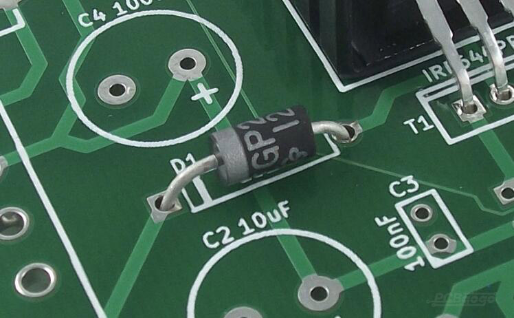
The markings on the silkscreen layer fulfill several vital functions that underpin successful PCB production and operation. During the assembly phase, precise reference designators and polarity indicators prevent misplacement of components, which is a common source of electrical malfunction. For instance, correctly identifying the anode and cathode of a diode or the orientation of an integrated circuit (IC) is made straightforward by clear silkscreen symbols.
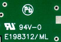
In the subsequent testing and maintenance stages, the silkscreen becomes an invaluable troubleshooting aid. Engineers and technicians can quickly locate specific components, test points, or critical areas on the board, significantly streamlining the diagnostic process. Beyond practical utility, the silkscreen also carries important regulatory and branding information. Symbols like RoHS (Restriction of Hazardous Substances), CE (Conformité Européenne), or UL (Underwriters Laboratories) ensure that the board adheres to essential industry standards and safety certifications. Additionally, company logos and part numbers reinforce the manufacturer's identity and facilitate inventory management.
What are the key elements of effective silkscreen design?
Crafting an effective silkscreen layer requires careful attention to several fundamental design principles. The primary goals are to ensure maximum legibility, strategic placement that avoids interference, and strict adherence to established industry guidelines.
Optimizing font, line, and placement for clarity
Legibility begins with the judicious selection of font size and line width. Text that is too small or lines that are too fine can easily become unreadable during manufacturing, especially under varying lighting conditions or if there are slight imperfections in the printing process. Industry best practices recommend a minimum font height of 0.035 inches (0.89 mm) for reference designators, with 0.050 inches (1.27 mm) being preferred for optimal readability. For larger markings like part numbers or company logos, fonts up to 0.080 inches can be used. The line width for silkscreen elements should be at least 0.006 inches (0.15 mm) to ensure the ink prints distinctly without smudging. Simple, non-serif font styles, such as Arial or Helvetica, are generally preferred over complex or decorative fonts, which can become distorted during the printing process.
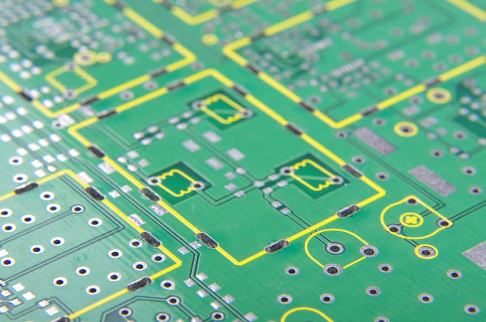
Strategic placement is equally critical to prevent conflicts with other PCB features. Silkscreen elements must maintain a minimum clearance, typically 0.005 inches (0.127 mm), from exposed conductive areas such as solder pads, vias, or traces. Placing silkscreen directly over solder pads can hinder component soldering, while overlapping vias might obscure their function. For high-speed signal lines, silkscreen ink can subtly alter the dielectric properties, leading to impedance discontinuities and potential signal degradation, so it should be kept clear of such critical paths. Furthermore, reference designators and polarity markers should always be positioned close to their respective components and remain visible even after assembly. For instance, a diode's cathode symbol should be immediately adjacent to its cathode pin to prevent incorrect orientation.
Importance of orientation, consistency, and color
Consistent orientation of text and markings significantly improves readability and reduces potential confusion during assembly. The general rule is to align all text to be read from left to right or from bottom to top of the board, minimizing unnecessary board rotation for technicians. Limiting text rotation to 0° or 90° further enhances clarity. It's also vital to match the silkscreen orientation of components to their respective datasheets, ensuring that Pin 1 markers for ICs, for example, accurately reflect the physical orientation to prevent installation errors.
Uniformity in naming conventions (e.g., using "R" for all resistors, "C" for all capacitors) and consistent labeling directions across the board are crucial for reducing ambiguity. The choice of silkscreen color also impacts legibility and manufacturability. White is the most common color, offering excellent contrast against standard green solder masks. Other colors like yellow, black, or red are available but may have varying manufacturing compatibility; for instance, pink silkscreen is often discouraged due to poor adhesion properties. Ultimately, selecting a color that provides high contrast against the solder mask ensures optimal visibility, while using a durable, non-conductive epoxy ink guarantees resistance to corrosion and high temperatures during soldering and operation.
Which industry standards govern PCB silkscreen design?
Adhering to established industry standards is not merely a recommendation but a necessity for ensuring that PCB silkscreen designs are compatible with manufacturing processes and meet essential regulatory requirements. These guidelines are crucial for quality, reliability, and global market access.
Key IPC and regulatory compliance standards
The Institute of Printed Circuits (IPC) provides a comprehensive set of guidelines that significantly influence PCB design, including specific criteria for silkscreen legibility and placement. IPC-A-600, for example, details acceptable conditions for all types of PCB board markings, stipulating minimum legibility requirements to ensure text and symbols remain readable even after manufacturing processes like reflow soldering. IPC-2221 offers recommendations for minimum clearances between silkscreen features and conductive elements, a crucial aspect for preventing manufacturing defects such as ink bridging or solderability issues. Furthermore, IPC-7351 defines standard component footprints, explicitly including guidelines for silkscreen markings that indicate polarity and pin identifiers, which are vital for correct component assembly.
Beyond these fundamental design standards, specific industries or markets often demand additional regulatory markings on the silkscreen. The RoHS (Restriction of Hazardous Substances) symbol is commonly used to indicate compliance with lead-free component requirements. For safety-certified boards, particularly in sectors like industrial or medical devices, a UL (Underwriters Laboratories) logo from a certified manufacturer might be mandatory, typically referencing UL 796/94 standards. Similarly, common in consumer electronics, CE (Conformité Européenne) and FCC (Federal Communications Commission) markings denote compliance with European and U.S. regulatory standards, respectively. Adhering to these standards ensures not only the functional integrity of the PCB but also its legal and commercial viability.
What are the common methods for printing PCB silkscreen?
The precision and legibility of the final silkscreen layer are heavily influenced by the printing method employed. Each technique offers different resolutions, pcb board cost, and suitability for various production volumes and design complexities.
Overview of primary silkscreen printing techniques
One of the most traditional methods is manual screen printing. In this technique, a non-conductive epoxy ink is pushed through a fine mesh stencil directly onto the PCB surface. While cost-effective for low-volume production runs or prototyping, manual screen printing typically offers a limited resolution, usually around 0.007 inches (0.18 mm), which can be insufficient for highly dense or intricate designs with very fine text.
For more complex designs requiring higher precision, Liquid Photo Imaging (LPI) is a widely adopted method. LPI utilizes a photosensitive ink that is applied to the entire PCB surface. This coated board is then exposed to UV light through a photomask, which transfers the silkscreen pattern. The unexposed ink is subsequently washed away, leaving only the desired markings. LPI provides significantly higher resolution, often down to 0.004 inches, making it ideal for boards with tighter component pitches and finer text requirements.
The most advanced technique is Direct Legend Printing (DLP). This method employs specialized inkjet printers that precisely apply the ink directly onto the PCB surface, much like a conventional inkjet printer. DLP offers the highest level of precision and resolution, capable of reproducing extremely fine text and intricate graphical elements. Consequently, it is the preferred method for high-density boards, compact IoT devices, or any application where precise, sharp, and highly legible silkscreen is paramount, even with very small font sizes.
Best practices for optimizing silkscreen design
To ensure a PCB silkscreen layer that is both highly legible and functionally effective, while also being compatible with manufacturing processes, designers should adopt a set of best practices. These guidelines help to strike a balance between clarity, usability, and manufacturability.
Practical tips for effective silkscreen implementation
When designing a silkscreen, especially for space-constrained boards, it is crucial to prioritize critical information. Essential markings like regulatory symbols, polarity indicators, and component reference designators should take precedence over less critical elements such as decorative logos or extensive branding, which can be placed strategically or scaled down. Before finalizing the design, it's highly recommended to print the PCB layout at its actual size. This physical printout should then be reviewed under various lighting conditions to assess legibility. Seeking feedback from colleagues or technicians can provide valuable insights into potential readability issues that might be overlooked.
Proactive communication with your PCB manufacturer is also a key practice. Confirm their specific silkscreen capabilities, including minimum achievable line widths, supported font sizes, and available ink colors, to avoid design choices that could lead to production delays or increased costs. Leveraging professional Electronic Design Automation (EDA) software, such as Altium Designer or Cadence Allegro, can significantly streamline the process. These tools often include intelligent auto-silkscreen features that automatically adjust text placement to prevent overlaps and ensure compliance with industry standards. Finally, for silkscreen elements intended for the bottom side of the PCB, ensure that these markings are correctly mirrored in the Gerber files. This ensures that when the board is viewed from the bottom, the text and symbols appear in the correct orientation, preventing assembly confusion.
The importance of optimized silkscreen for PCB reliability
A meticulously designed PCB silkscreen layer is more than just an aesthetic detail; it is a fundamental component that underpins efficient manufacturing, simplifies assembly, and contributes significantly to the long-term reliability of electronic products. By prioritizing legibility through careful selection of font sizes, precise placement that avoids critical areas, and the use of high-contrast colors, engineers can create boards that are intuitively easy to work with. Adhering to recognized industry standards, such as those set by IPC, and complying with specific regulatory requirements, further solidifies the integrity and market acceptance of the design.
As printed circuit boards continue to shrink in size and grow in complexity, the role of mastering silkscreen design becomes increasingly vital. It ensures that critical information remains clear and accessible, even on crowded boards. By consistently following the guidelines and incorporating the best practices outlined in this discussion—including early consultation with manufacturers, strategic use of professional design tools, and a clear prioritization of critical information—designers can significantly optimize their silkscreen layers. This diligent approach ultimately ensures that their PCBs perform flawlessly in real-world applications, offering both operational efficiency and enduring reliability.


