Introduction
The dry film solder mask exposure process is a critical step in printed circuit board (PCB) manufacturing. It ensures the protective layer on a PCB is applied with precision, safeguarding copper traces from environmental damage and preventing solder bridges during assembly. For electrical engineers, mastering this process can significantly enhance board reliability and performance. This tutorial explores dry film solder mask exposure settings, UV exposure techniques, optimal exposure times, necessary equipment, and troubleshooting methods. By understanding these elements, engineers can achieve consistent results and minimize defects in production. The guidance provided here aligns with recognized industry standards to support professionals in optimizing their workflow.
What Is Dry Film Solder Mask and Why It Matters
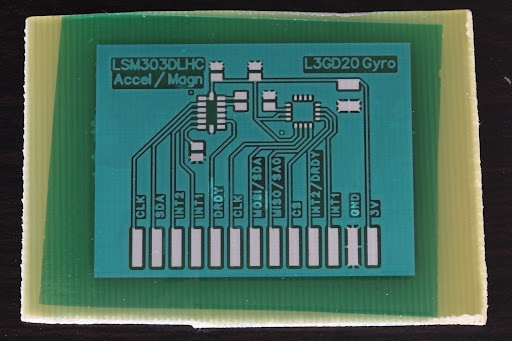
Dry film solder mask is a thin polymer layer applied to PCBs to protect copper traces and define areas for soldering. Unlike liquid photoimageable masks, dry film comes in a roll or sheet form, laminated onto the board before exposure. This method offers uniformity and is widely used in high volume production for its efficiency. The exposure process uses ultraviolet (UV) light to harden specific areas of the mask, creating a durable barrier after development.
The importance of this process lies in its impact on PCB quality. A properly exposed solder mask prevents oxidation, insulates traces, and ensures accurate component placement. Errors in exposure can lead to incomplete coverage, misalignment, or weak adhesion, compromising the board's functionality. For electrical engineers, precise control over this step is essential to meet design specifications and maintain reliability in demanding applications.
Technical Principles of Dry Film Solder Mask Exposure
The exposure process relies on photochemical reactions. Dry film solder mask contains photoinitiators that react to UV light, typically in the 350 to 400 nanometer wavelength range. When exposed, the illuminated areas polymerize and harden, while unexposed regions remain soluble and are later removed during development. This selective hardening defines the mask pattern based on the artwork or photomask used.
Key factors influencing the process include UV light intensity, exposure time, and the alignment of the photomask. Insufficient light intensity or time may result in under exposure, leaving parts of the mask unhardened. Conversely, overexposure can cause unwanted hardening beyond the intended areas, leading to pattern distortion. The photomask must be precisely aligned with the board to avoid misregistration, which can expose incorrect areas or leave critical traces unprotected.
Temperature and humidity also play roles in the process. Elevated temperatures can affect the film's sensitivity, while high humidity might cause adhesion issues before exposure. Controlling these environmental conditions ensures consistent outcomes. Engineers must adhere to guidelines set by standards such as IPC-6012E, which outlines performance specifications for rigid printed boards, including solder mask application.
Dry Film Solder Mask Exposure Settings and Best Practices
Achieving optimal results requires careful adjustment of dry film solder mask exposure settings. While specific values depend on the film type and equipment, general principles apply. UV exposure units typically operate with mercury vapor lamps or LED sources, delivering consistent light output. Engineers should consult the film manufacturer's datasheet for recommended energy levels, often measured in millijoules per square centimeter.
Exposure time is another critical parameter. For many dry films, exposure times range from a few seconds to a minute, based on light intensity. A common practice is to perform test exposures on scrap boards to determine the ideal duration. This approach helps balance under and overexposure risks, ensuring the mask fully protects designated areas without pattern bleed.
Alignment accuracy is vital for dry film solder mask UV exposure. Photomasks or artwork must match the board's layout precisely. Using registration pins or optical alignment systems can minimize errors. Additionally, the exposure unit's vacuum frame should hold the board and photomask tightly to prevent movement during the process. Following standards like IPC-A-600K for acceptability of printed boards ensures the final mask meets quality criteria.
Dry Film Solder Mask Exposure Time Optimization
Determining the correct dry film solder mask exposure time is essential for process reliability. Insufficient time results in incomplete polymerization, leading to mask defects during development. Excessive time can harden areas outside the desired pattern, causing issues like reduced clearance between pads. A practical method to optimize time involves using a step wedge or exposure test strip, which features varying opacity levels to gauge the film's response to different durations.
Environmental factors must be monitored during this optimization. Ambient temperature should remain stable, as fluctuations can alter the film's sensitivity to UV light. Humidity control is equally important to prevent moisture from affecting film adhesion before exposure. Engineers should document test results to establish a repeatable process, aligning with quality management principles in ISO 9001:2015.
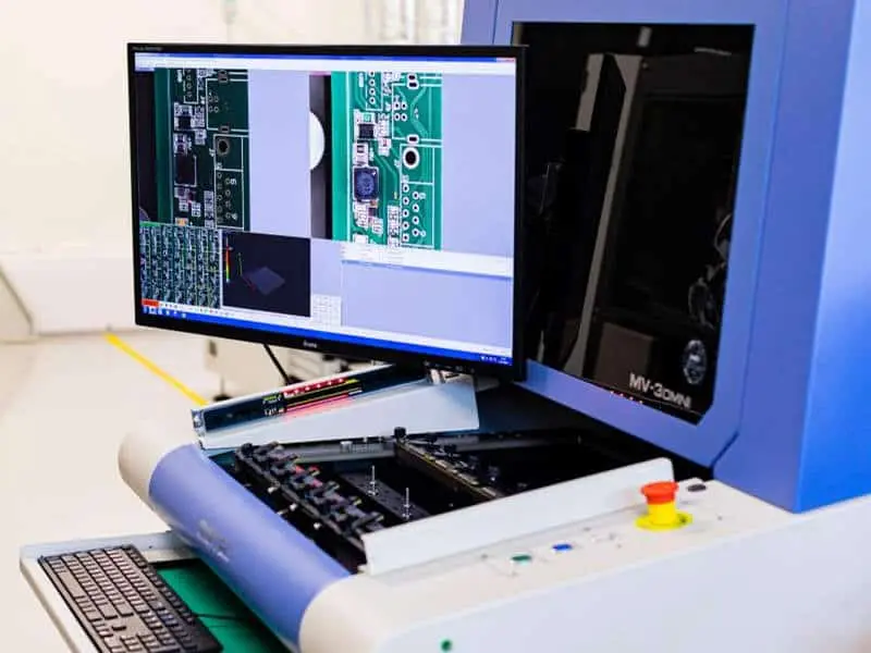
Dry Film Solder Mask Exposure Equipment Essentials
Selecting appropriate dry film solder mask exposure equipment is crucial for consistent outcomes. Exposure units vary from tabletop models for prototyping to large scale systems for production. Key features to consider include light source uniformity, vacuum frame capability, and timer accuracy. Uniform light distribution prevents hotspots that could cause uneven exposure, while a strong vacuum ensures tight contact between the board and photomask.
Maintenance of equipment is equally important. Regular calibration of light intensity and replacement of aging lamps maintain performance. Cleanliness of the exposure area prevents dust or debris from interfering with the photomask contact. Engineers should follow equipment guidelines and industry standards such as IPC-6012E to ensure the setup supports high quality solder mask application.
Troubleshooting Dry Film Solder Mask Exposure Issues
Even with careful preparation, issues can arise during the exposure process. Troubleshooting dry film solder mask exposure problems requires a systematic approach to identify and resolve root causes. Below are common challenges and solutions for electrical engineers.
- Under exposure: This occurs when the film does not fully harden, leading to mask loss during development. Check light intensity and increase exposure time incrementally. Verify the film's storage conditions, as aged or improperly stored film may lose sensitivity.
- Overexposure: Excessive UV light can harden unintended areas, reducing pattern accuracy. Reduce exposure time or light intensity. Ensure the photomask is clean and free of defects that might scatter light.
- Misalignment: If the mask pattern does not match the board layout, inspect the alignment process. Use registration aids and confirm the vacuum frame secures the board properly.
- Adhesion Failure: Poor film adhesion before exposure often results from surface contamination or high humidity. Clean the board thoroughly and control environmental conditions to improve contact.
Documenting troubleshooting efforts helps build a knowledge base for future reference. Adhering to standards like IPC-A-600K provides a framework for evaluating and correcting solder mask defects.
Practical Insights for Electrical Engineers
For engineers working on complex designs, integrating the exposure process into the broader manufacturing workflow is essential. Coordination with upstream processes like board cleaning and lamination ensures the surface is ready for film application. Post exposure steps, including development and curing, should follow precise protocols to lock in the mask's protective properties.
Testing small batches before full production runs can prevent costly errors. Using control charts or statistical process control methods, as outlined in ISO 9001:2015, supports consistent quality. Engineers should also stay updated on advancements in exposure technology, such as LED based UV systems, which offer energy efficiency and precise control over light output.
Related Reading: The Ultimate Guide to Selecting the Right Dry Film Solder Mask Thickness for Optimal PCB Performance
Conclusion
Mastering the dry film solder mask exposure process is a foundational skill for electrical engineers involved in fast turn circuit board manufacturing. By understanding the technical principles, optimizing exposure settings, selecting appropriate equipment, and addressing common issues, professionals can achieve reliable and high quality results. Attention to factors like UV exposure time and environmental control further enhances outcomes. Following industry standards ensures compliance with best practices, supporting the production of durable and functional boards for diverse applications.
FAQs
Q1: What are the ideal dry film solder mask exposure settings for consistent results?
A1: Achieving consistent results with dry film solder mask exposure settings involves balancing UV light intensity and duration. Test exposures on scrap boards help determine optimal settings based on film type. Maintain stable temperature and humidity to avoid sensitivity issues. Following guidelines from standards like IPC-6012E ensures the process aligns with industry expectations for rigid board performance.
Q2: How does dry film solder mask UV exposure impact PCB reliability?
A2: Dry film solder mask UV exposure directly affects PCB reliability by defining the protective layer over copper traces. Proper exposure prevents oxidation and solder bridges, ensuring electrical integrity. Incomplete or excessive exposure can lead to defects, compromising insulation. Adhering to precise exposure protocols is vital for long term board performance in demanding environments.
Q3: What factors influence dry film solder mask exposure time during production?
A3: Dry film solder mask exposure time is influenced by UV light intensity, film sensitivity, and environmental conditions. Higher intensity shortens required time, while aged film may need longer exposure. Temperature and humidity fluctuations can alter outcomes. Testing with step wedges helps establish the correct duration for consistent polymerization across production runs.
Q4: How can engineers troubleshoot dry film solder mask exposure defects effectively?
A4: To troubleshoot dry film solder mask exposure defects, engineers should systematically check for under or overexposure, misalignment, and adhesion issues. Adjust exposure time and light intensity as needed. Ensure proper board cleaning and photomask alignment. Document findings to refine the process, and refer to standards like IPC-A-600K for acceptable quality benchmarks.
References
IPC-6012E — Qualification and Performance Specification for Rigid Printed Boards. IPC, 2020.
IPC-A-600K — Acceptability of Printed Boards. IPC, 2020.
ISO 9001:2015 — Quality Management Systems. ISO, 2015.


