Introduction
Thermal management in LED lighting PCB design is a critical factor for ensuring performance, reliability, and longevity of electronic systems. LEDs, while energy-efficient, generate significant heat at the junction, which can degrade efficiency and lifespan if not managed properly. For electrical engineers, understanding how to address heat dissipation through effective design strategies is essential. This guide explores key aspects of thermal management, including the use of thermal vias, heat sink integration, and appropriate material selection. By focusing on concepts like LED junction temperature control and PCB material thermal resistance, this article provides actionable insights. Whether designing high-power LED systems or compact lighting solutions, mastering these principles ensures optimal operation and durability in demanding applications.
Why Thermal Management Matters in LED PCB Design
Effective thermal management is vital in LED lighting systems due to the heat generated during operation. High temperatures at the LED junction can reduce light output, shift color, and shorten component life. For electrical engineers, the challenge lies in dissipating this heat to maintain performance within safe limits. Poor thermal design can lead to system failures, increased maintenance costs, and compromised safety in applications like automotive or industrial lighting. By prioritizing heat dissipation strategies, such as integrating thermal vias and selecting suitable materials, designers can enhance reliability. This not only protects the LEDs but also ensures consistent operation in varied environments. Understanding thermal resistance paths and simulation techniques is key to achieving these goals in PCB layouts.
Related Reading: Beyond FR 4: Exploring Advanced PCB Materials for High Performance LED Lighting
Technical Principles of Thermal Management in LED PCBs
Understanding LED Junction Temperature
The junction temperature of an LED is the operating temperature at the semiconductor junction where light is produced. Elevated temperatures at this point directly impact efficiency and lifespan. Industry standards, such as those from JEDEC, emphasize maintaining junction temperatures within specified limits to prevent thermal runaway. Heat must be conducted away from this point through the PCB and other components to avoid degradation. Engineers must calculate the thermal path resistance to predict and control this temperature during design phases.
PCB Material Thermal Resistance and Selection
The choice of PCB material significantly affects thermal performance. Materials with low thermal resistance facilitate better heat transfer from the LED to the ambient environment. Standard FR-4 materials often have higher thermal resistance, making them less suitable for high-power LED applications. Metal-core PCBs (MCPCBs), with aluminum or copper bases, offer superior thermal conductivity. Selecting materials based on thermal conductivity values and dielectric properties ensures efficient heat dissipation. This selection process must align with guidelines like IPC-6012E for rigid board performance specifications.
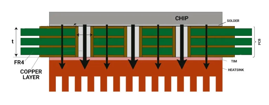
Role of Thermal Vias in Heat Dissipation
Thermal vias are small, plated-through holes in a PCB that create low-resistance paths for heat to travel from the top layer to the bottom or internal layers. They are crucial in LED PCB designs to transfer heat away from the LED junction. Placing thermal vias directly beneath or near the LED mounting area enhances heat conduction to a heat sink or other cooling mechanisms. The effectiveness depends on via density, diameter, and placement, which should follow best practices outlined in industry standards like IPC-A-600K for PCB acceptability.
Related Reading: Mastering Thermal Vias: Essential Heat Management for High-Power PCBs
Heat Sink Design for PCBs
Integrating a heat sink into LED PCB designs is a common method to manage heat. A heat sink absorbs and dissipates thermal energy through convection to the surrounding air. Its design must consider surface area, material (often aluminum for cost and conductivity), and mounting to the PCB. Proper alignment with thermal vias ensures an efficient heat transfer path. Engineers must balance size and weight with thermal performance to meet application needs without overcomplicating the layout.
Thermal Interface Materials for LEDs
Thermal interface materials (TIMs) bridge the gap between the LED, PCB, and heat sink, reducing thermal resistance at contact points. These materials, such as thermal greases or pads, improve heat transfer by filling microscopic air gaps. Selection criteria include thermal conductivity, thickness, and application method. TIMs must maintain stability under operating temperatures to ensure long-term reliability. Their role is critical in maintaining low junction temperatures and must be chosen based on performance requirements.
Practical Solutions for Effective Thermal Management
Optimizing Thermal Vias Placement and Density
To maximize the effectiveness of thermal vias in LED PCBs, strategic placement is essential. Vias should be positioned directly under or adjacent to the LED thermal pad to create the shortest heat conduction path. Increasing via density in high-heat areas improves thermal performance, but over-density can weaken the PCB structure. A balance must be struck, adhering to manufacturing constraints outlined in standards like IPC-A-600K. Using simulation tools during the design phase helps identify optimal via configurations.
Designing Efficient Heat Sinks
Heat sink design for PCBs requires careful consideration of geometry and material. Finned structures increase surface area for better convection, while materials with high thermal conductivity enhance heat transfer. Mounting the heat sink securely to the PCB ensures minimal thermal resistance at the interface. Engineers should also account for airflow in the application environment to maximize cooling efficiency. Testing different designs under operating conditions validates their performance before final implementation.
Selecting Thermal Interface Materials
Choosing the right thermal interface materials for LEDs involves evaluating thermal conductivity and compatibility with the application. Thin layers of high-conductivity materials reduce resistance, but application ease and durability are equally important. Engineers must ensure the material withstands thermal cycling without degrading. Standards like JEDEC J-STD-020E provide guidance on material behavior under stress, aiding in selection. Proper application techniques prevent air gaps, ensuring consistent heat transfer.
Leveraging PCB Material Choices
Using materials with low thermal resistance is a foundational step in LED PCB design. Metal-core substrates, often preferred for high-power applications, offer excellent heat dissipation compared to standard laminates. Engineers must weigh cost against performance when selecting materials. Layer stack-up design also influences thermal paths, with internal copper planes acting as heat spreaders. Following IPC-6012E ensures material choices meet performance and reliability standards for rigid boards.
Implementing PCB Thermal Simulation
PCB thermal simulation is a powerful tool for predicting heat distribution and identifying hotspots before manufacturing. Simulation software models heat flow through vias, materials, and interfaces, providing insights into junction temperature behavior. Engineers can test various design iterations virtually, optimizing layouts for thermal performance. Accurate input data, such as material properties and boundary conditions, is critical for reliable results. This approach reduces design iterations and ensures compliance with thermal limits.

Troubleshooting Common Thermal Issues in LED PCBs
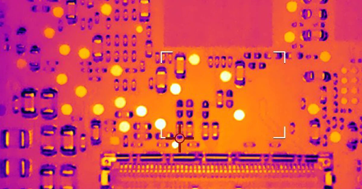
Identifying Hotspots and Failures
Hotspots in LED PCBs often result from inadequate heat dissipation paths or poor via placement. These areas can cause elevated LED junction temperatures, leading to reduced efficiency or failure. Engineers can use thermal imaging during testing to locate hotspots and correlate them with simulation data. Addressing these issues may involve adding thermal vias or adjusting component placement. Consistent monitoring during prototyping helps prevent long-term reliability problems.
Mitigating Thermal Resistance
High thermal resistance in the PCB stack-up or at interfaces hinders heat transfer. Reducing resistance involves selecting materials with better conductivity and ensuring tight contact between components and heat sinks. Thermal interface materials play a key role here, as do proper mounting techniques. Reviewing designs against standards like IPC-A-600K ensures manufacturing quality does not introduce additional resistance. Iterative testing and simulation refine these solutions effectively.
Managing High-Power Applications
High-power LED systems generate substantial heat, demanding robust thermal management. Combining multiple strategies, such as dense thermal vias, large heat sinks, and advanced materials, addresses this challenge. Engineers must also consider ambient conditions and enclosure design to facilitate cooling. Simulation tools help predict performance under peak loads, guiding design adjustments. Adhering to industry guidelines ensures the system operates safely under stress.
Conclusion
Mastering thermal management in LED lighting PCB design is essential for ensuring performance and reliability. By understanding key concepts like LED junction temperature and PCB material thermal resistance, engineers can create effective heat dissipation strategies. Practical solutions, including thermal vias, heat sink design, and thermal interface materials, provide actionable ways to address heat challenges. Leveraging tools like PCB thermal simulation further optimizes designs for real-world conditions. Following industry standards and best practices ensures consistent results, extending the lifespan of LED systems. This comprehensive thermal design guide equips engineers with the knowledge to tackle thermal issues confidently.
FAQs
Q1: How do thermal vias improve LED PCB thermal management?
A1: Thermal vias create low-resistance paths for heat to move from the LED junction to cooler areas of the PCB or a heat sink. By placing them strategically under LED components, engineers ensure efficient heat dissipation. Their density and size must balance thermal performance with structural integrity. Following industry standards for via design prevents manufacturing issues while enhancing reliability in high-heat applications.
Q2: What factors influence heat sink design for PCBs in LED lighting?
A2: Heat sink design for PCBs depends on material conductivity, surface area, and application environment. Aluminum is often used for its balance of cost and performance. Finned structures improve convection, while secure mounting reduces thermal resistance. Airflow in the system also impacts cooling efficiency. Engineers must tailor designs to specific power levels and space constraints for optimal results.
Q3: Why is LED junction temperature critical in PCB design?
A3: LED junction temperature directly affects light output, color accuracy, and component lifespan. High temperatures reduce efficiency and can cause premature failure. Effective thermal management, through vias and heat sinks, keeps this temperature within safe limits. Engineers must calculate thermal paths and use simulation to predict behavior. Maintaining low junction temperatures ensures consistent performance in demanding LED applications.
Q4: How does PCB material thermal resistance impact thermal design?
A4: PCB material thermal resistance determines how effectively heat transfers from the LED to the environment. High-resistance materials like standard FR-4 hinder dissipation, while metal-core substrates excel in high-power designs. Selecting materials with low resistance improves thermal performance. Engineers must align choices with application needs and industry standards to ensure reliability and efficiency in LED systems.
References
IPC-6012E — Qualification and Performance Specification for Rigid Printed Boards. IPC, 2020.
IPC-A-600K — Acceptability of Printed Boards. IPC, 2020.
JEDEC J-STD-020E — Moisture/Reflow Sensitivity Classification. JEDEC, 2014.


