What Are Thermal Vias and Why Are They Crucial for High-Power PCBs?
As electronic devices continue to shrink in size while simultaneously increasing in power, the effective management of heat dissipation within printed circuit boards (PCBs) has emerged as a formidable challenge for design engineers. High-power components, such as sophisticated processors, high-brightness LEDs, and efficient power regulators, generate substantial amounts of heat. Without precise thermal management, this heat accumulation can lead to significant performance degradation, drastically shorten component lifespans, or even result in complete system failure. Among the most effective solutions employed in contemporary PCB design is the strategic use of thermal vias—small, highly conductive pathways specifically engineered to channel heat away from localized hot spots to cooler regions of the board. This exploration delves into the scientific principles underpinning thermal vias, critical design considerations, and practical strategies for optimizing heat dissipation in high-power PCBs.
For engineers engaged in cutting-edge applications—ranging from complex aerospace systems and advanced automotive electronics to high-performance computing platforms—a deep understanding of how to effectively implement thermal vias can be the decisive factor between developing a robust, reliable product and facing costly redesigns. These seemingly minor features exert a significant influence on thermal management, proving that even tiny elements can deliver substantial impact.
Defining Thermal Vias and Their Purpose
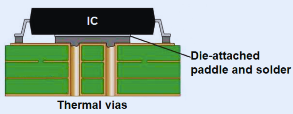
A thermal via is a plated through-hole (PTH) primarily engineered for its thermal conductivity rather than for electrical signal transmission. These vias are typically either filled or lined with copper, a material renowned for its high thermal conductivity (approximately 385 W/m·K), which vastly surpasses that of standard FR4 substrate (around 0.3 W/m·K). Functionally, thermal vias behave much like miniature heat pipes. Their core purpose is to efficiently conduct heat away from the thermal pad of a high-power component and transfer it to a larger copper plane, a dedicated heat sink, or even to the opposing side of the PCB where convection and radiation can effectively dissipate the heat into the ambient air.
A key distinction between thermal vias and signal vias lies in their primary focus: signal vias prioritize electrical performance, impedance control, and precise trace routing, whereas thermal vias are optimized for low thermal resistance and highly efficient heat conduction.
The Significance of Thermal Vias in Modern Electronics
In high-power PCB environments, components can frequently reach temperatures well over 100°C, significantly exceeding the safe operating limits for most electronic parts, which are typically around 85°C for standard components. Excessive heat is a major culprit in reducing a component's operational lifespan; according to the Arrhenius equation, a component's life can be halved for every 10°C increase beyond its rated temperature. Thermal vias are instrumental in mitigating this issue by effectively spreading heat across the entire board, thereby preventing the formation of localized hot spots that could compromise the overall reliability and longevity of the electronic system.
Understanding the Scientific Principles Behind Thermal Via Operation
Heat dissipation within PCBs fundamentally relies on three core mechanisms: conduction, convection, and radiation. Thermal vias predominantly enhance conduction—the process by which heat is transferred through a solid material. When a high-power component, such as a MOSFET, generates heat, this energy initially flows into the copper pad located beneath it. Without the presence of thermal vias, this heat would largely remain trapped near the surface due to the inherently low thermal conductivity of standard PCB substrates like FR4. Thermal vias ingeniously bridge this thermal gap by establishing a vertical pathway that directs heat to a larger copper plane or a heat sink, where the heat can then spread out and dissipate much more effectively into the surrounding environment.
The overall effectiveness of thermal vias is influenced by several critical design and material factors:
● Copper Plating Thickness: A thicker copper layer (e.g., 1 oz/ft² or 35 µm) offers superior thermal conductivity compared to thinner layers (e.g., 0.5 oz/ft² or 17 µm).
● Via Diameter: Larger vias (e.g., 0.3 mm) are capable of conducting more heat than smaller ones (e.g., 0.1 mm), although they naturally require more board space.
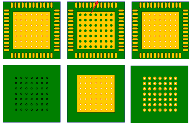
● Number of Vias: Thermal simulation studies have shown that employing an array of, for example, 6x6 vias beneath a component can reduce the junction temperature by as much as 4.8°C compared to using a single via.
● Strategic Placement: Positioning thermal vias directly underneath the primary heat source is crucial for maximizing their efficiency.
By creating a direct thermal link to a ground plane or a dedicated heat sink, thermal vias also facilitate efficient horizontal heat spreading. This leverages the extensive surface area of the copper to enhance both convection and radiation of heat into the ambient air, further improving the overall thermal performance of the PCB.
Essential Design Considerations for Optimizing Thermal Via Performance
Integrating thermal vias effectively into a high-power PCB design demands more than just drilling a few holes; engineers must meticulously balance thermal efficiency with electrical integrity, manufacturing feasibility, and cost constraints. Here are some pivotal design considerations.
Optimizing Via Size and Spacing
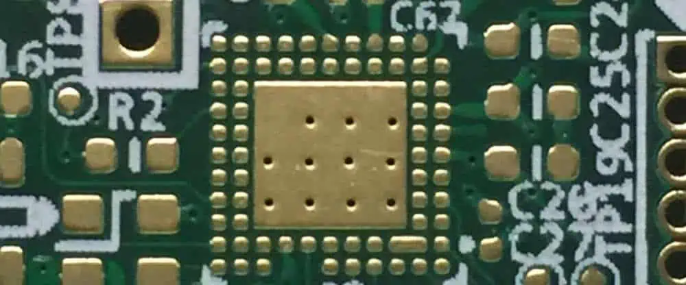
Smaller vias, typically ranging from 0.1–0.3 mm in diameter, enable a higher density of placement, allowing more thermal pathways to be fitted beneath a single component. Conversely, larger vias, due to their greater cross-sectional area, can transfer heat more effectively individually. A common and balanced approach involves utilizing an array of smaller vias—for instance, 16 vias arranged in a 4x4 grid—with approximately 1 mm spacing between them. This configuration optimizes heat transfer while making efficient use of board real estate. Spacing vias too closely can compromise the structural integrity of the board, while spacing them too far apart will diminish the effectiveness of heat transfer.
Selecting Appropriate Via Filling Options
Unfilled vias offer a cost-effective solution but carry the risk of solder wicking into the barrel during assembly, which can reduce their effective thermal contact. Filled vias, on the other hand, are either capped with copper or plugged with a thermally conductive epoxy. This prevents solder wicking, significantly improves heat conduction, and is particularly beneficial for boards thicker than 0.7 mm, where filled vias placed directly under a thermal pad can reduce thermal resistance by up to 20%.
Strategic Connection to Copper Planes
Thermal vias achieve maximum effectiveness when they are directly connected to a large copper plane, such as a ground layer. This plane functions as an efficient heat spreader, distributing thermal energy across a much wider area. It is generally advisable to avoid using thermal relief patterns (spokes) around thermal vias unless ease of soldering is a primary concern, as these patterns inherently increase thermal resistance by limiting direct copper contact.
Precision in Via Placement Strategy
The most effective placement strategy for thermal vias is directly beneath or in very close proximity to the primary heat source, such as the thermal pad of a QFN package. For larger components, strategically placing additional vias around the periphery can further enhance heat dissipation. Thermal simulations reveal that a 6x6 via array under a 2.5W device can lower the junction temperature by 4.8°C, while a 4x4 array increases it by 2.2°C—these seemingly minor temperature differences can be critical in high-power designs.
Troubleshooting and Diverse Applications of Thermal Vias
Even meticulously designed thermal via configurations may require adjustments during development or post-production. Understanding common issues and the broad applicability of thermal vias is crucial.
Troubleshooting Thermal Via Effectiveness
To troubleshoot thermal management issues related to vias, engineers should:
● Identify Hot Spots: Utilize thermal imaging cameras or infrared (IR) sensors to precisely pinpoint areas of excessive heat on the PCB.
● Analyze Via Configuration: Evaluate the density of thermal vias and their connectivity to copper planes.
● Inspect Manufacturing Quality: Check for potential defects such as incomplete plating, improper via filling, or poor soldering that might impede thermal flow.
● Reevaluate Layout: Assess the overall PCB layout to ensure that sufficient copper area and via coverage are provided for heat spreading.
● Perform Thermal Simulations: Employ advanced tools like Cadence or Altium's thermal solvers to model heat flow and predict temperature distributions under various operating conditions.
Real-World Applications Across Industries
● High-Brightness LEDs: Over 60% of the electrical energy consumed by high-power LEDs is converted into heat. Without robust thermal management, this heat can drastically reduce light output and shorten the LED's operational life. Thermal vias efficiently channel heat from the LED pad to underlying copper planes or metal cores, thereby sustaining optimal performance and longevity.
● Retail Technology: Electronic devices in retail environments, including point-of-sale (POS) terminals, barcode scanners, and digital signage, often operate continuously for extended periods, generating substantial internal heat. Correct thermal via placement ensures consistent, reliable operation and prevents thermal throttling in sensitive internal electronics.
● Aerospace & Automotive Systems: In environments characterized by extreme temperatures and demanding operational conditions, robust thermal management is critical. Here, advanced solutions such as filled Via-in-Pad Plated Over (VIPPO) vias and metal-core PCBs are frequently employed to meet stringent reliability requirements.
Benefits, Challenges, and Practical Implementation of Thermal Vias
Thermal vias offer distinct advantages but also come with trade-offs. Effective implementation requires balancing these factors with project needs.
Advantages of Integrating Thermal Vias
Thermal vias provide several advantages that make them indispensable in high-power applications:
● Enhanced Reliability: By maintaining component temperatures below critical thresholds (e.g., 85°C), thermal vias significantly extend the operational lifespan of electronic components.
● Cost-Effective Cooling Solution: Unlike external heat sinks or cooling fans, thermal vias are integrated within the HDI PCB itself, adding no extra parts and thereby reducing assembly complexity and overall cost.
● Space Efficiency: Thermal vias fit within the existing PCB footprint, making them an ideal thermal management solution for compact designs such as wearables or Internet of Things (IoT) devices.
● Optimized Performance: Lower operating temperatures prevent thermal throttling in processors and high-power LEDs, ensuring they operate at their peak efficiency and performance levels.
Challenges and Limitations
Despite their powerful capabilities, thermal vias are not without trade-offs:
● Manufacturing Complexity: The fabrication of filled or capped vias increases the overall cost of custom PCBs and demands precise manufacturing processes to avoid defects.
● Potential Electrical Interference: Connecting numerous thermal vias directly to a ground plane can introduce parasitic capacitance, which may affect the integrity of high-frequency PCB signals.
● Limited Heat Dissipation Capacity: In scenarios involving extremely high-power components (e.g., those dissipating over 10W), thermal vias alone may be insufficient, necessitating supplementary cooling solutions such as external heat sinks or forced air circulation.
Engineers must carefully weigh these factors against the specific requirements of their application. For example, a high-frequency RF board might prioritize signal integrity over a dense array of thermal vias, whereas a power supply PCB would likely maximize the thermal via count.
Practical Steps for Implementing Thermal Vias
To effectively integrate thermal vias into your next high-power PCB project, consider these actionable steps:
1. Analyze Heat Sources: Consult manufacturer datasheets to identify components with significant power dissipation (e.g., greater than 1W) and their specific thermal pad requirements.
2. Early Simulation: Utilize thermal solvers in tools like Cadence or Altium to model heat flow. This allows you to predict how varying via counts and placements impact temperature. Aim to maintain a junction temperature at least 20°C below the maximum rated temperature.
3. Adhere to Guidelines: For QFN or DFN packages, strictly follow the datasheet recommendations, which typically suggest 9–25 vias arranged in a grid pattern.
4. Optimize Copper Layers: Pair thermal vias with thicker copper layers (e.g., 2 oz/ft²) to significantly improve lateral heat spreading.
5. Prototype Testing: Employ thermal imaging cameras to meticulously verify thermal performance and identify any unexpected hot spots on physical prototypes.
Advanced Techniques: Beyond Basic Thermal Via Implementation
For projects facing extreme thermal challenges, engineers can leverage advanced thermal via techniques to further enhance heat dissipation.
Cutting-Edge Thermal Management Solutions
● Microvias: In High-Density Interconnect (HDI) boards, stacked or staggered microvias can dramatically increase via density in confined spaces, offering superior localized heat transfer.
● Metal Core PCBs (MCPCBs): Combining thermal vias with an aluminum or copper core (thermal conductivity typically around 200 W/m·K) substantially boosts overall heat dissipation, making MCPCBs ideal for applications like high-power LEDs.
● Via-in-Pad Technology: Placing filled vias directly within a component's soldering pad minimizes thermal resistance at the heat source, a technique particularly effective for boards thicker than 1.6 mm.
These advanced techniques are especially valuable in demanding aerospace or automotive designs, where unwavering reliability under harsh operating conditions is an absolute imperative.
How AIVON Supports Thermal Management in PCB Design
For engineers undertaking high-power PCB projects, collaborating with a reliable and large PCB manufacturer is crucial for streamlining the development process. At AIVON, we provide advanced manufacturing capabilities, including precision via drilling and meticulous copper plating, to ensure that your thermal vias perform exactly as designed. Our quick-turn prototyping services enable rapid testing and validation of thermal management strategies, while our efficient global logistics guarantee timely delivery—a critical factor when iterating on heat-sensitive designs. Whether you are developing a compact IoT device or a robust power supply, our expertise helps transform your thermal via concepts into high-performing realities with exceptional precision and efficiency.
Conclusion: Mastering Thermal Vias for Reliable High-Power Electronics
Thermal vias represent a fundamental element of effective thermal management in high-power PCBs, offering a straightforward yet potent means to control operating temperatures. By thoroughly understanding their underlying mechanics, designing them with meticulous care, and pairing them with appropriate materials and tools, engineers can successfully create electronic systems that are not only highly reliable but also exceptionally high-performing. Every detail, from the selection of via size and optimal placement to the implementation of advanced techniques such as MCPCBs, plays a critical role in the ongoing battle against excessive heat.
As power densities continue to escalate and electronic designs become increasingly complex, thermal vias will remain an essential go-to solution. Begin integrating them into your upcoming projects, meticulously simulate their impact, and observe the tangible difference they make in product performance and longevity.


