Introduction
In high-voltage PCB designs, the choice of dielectric material directly influences the reliability and safety of the board. Electric engineers must consider how the dielectric withstands electric stress across spacing between conductors. Poor material selection can lead to tracking, arcing, or outright failure under operational voltages. This article explores high voltage PCB dielectric materials, focusing on key properties like the comparative tracking index (CTI). Understanding these factors helps optimize creepage and clearance distances while adhering to industry standards. Proper dielectric selection ensures compact designs without compromising performance.
Understanding Dielectric Materials in PCBs
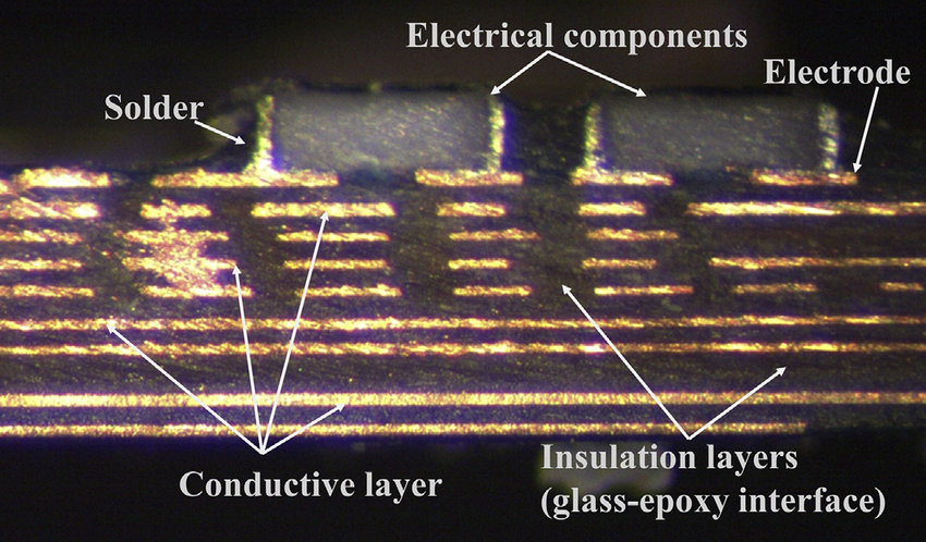
Dielectric materials in PCBs serve as insulators between conductive traces, preventing unintended current flow. These materials must exhibit high dielectric strength to handle voltage gradients without breakdown. In high-voltage applications, surface and volume properties become critical for maintaining spacing integrity. Common epoxy-based laminates dominate due to cost and processability, but their performance varies under stress. Engineers evaluate dielectric constant, loss tangent, and tracking resistance to match application needs. The dielectric's interaction with environmental factors like humidity amplifies the need for robust selection.
The Role of Comparative Tracking Index (CTI) in High-Voltage Applications
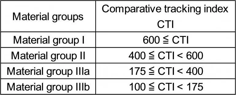
The comparative tracking index (CTI) quantifies a material's resistance to surface tracking, where conductive paths form along the dielectric surface due to contamination or voltage stress. Defined by IEC 60112, CTI measures the highest voltage at which the material withstands 100 drops of electrolyte solution without tracking. Higher CTI values indicate better insulation reliability in polluted environments. IPC-2221 uses CTI to classify materials into groups that dictate minimum creepage distances. For instance, materials fall into groups based on CTI thresholds, allowing designers to calculate spacing precisely. This parameter proves essential for high voltage PCB dielectric material choices in power electronics and industrial controls.
- Material Group I: ≥ 600 V
- Material Group II: 400 - 599 V
- Material Group IIIa: 175 - 399 V
- Material Group IIIb: 100 - 174 V
FR4 High Voltage Limitations
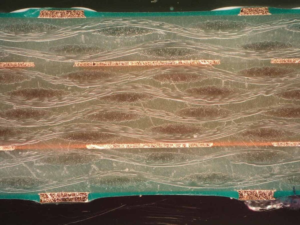
FR4, a standard epoxy glass laminate, offers good mechanical strength and moderate cost for general PCBs. However, FR4 high voltage limitations arise from its typical CTI around 175 V, placing it in Material Group IIIa. This restricts its use in applications exceeding a few hundred volts without excessive spacing. Surface porosity in FR4 can trap contaminants, accelerating tracking under high electric fields and humidity. While its bulk dielectric breakdown exceeds 40 kV/mm, surface effects dominate failures in high-voltage scenarios. Engineers often encounter partial discharges or corona in FR4 boards pushed beyond design limits, necessitating alternatives for voltages above 1 kV.
In practice, FR4 suits low to medium voltage designs but demands wider creepage distances per IPC-2221 tables for higher potentials. Upgrading to high-CTI FR4 variants improves performance marginally, yet inherent epoxy limitations persist. Testing reveals that FR4 degrades faster in harsh environments compared to specialized dielectrics. For electric engineers, recognizing these boundaries prevents field failures in power supplies or inverters.
Selecting the Best PCB Material for High Voltage
The best PCB material high voltage applications prioritize CTI above 400 V, alongside thermal stability and low moisture absorption. Epoxy resins with high filler content or modified formulations achieve Group II or I ratings, reducing required creepage by up to 50% versus FR4. Polyimide-based materials offer superior thermal endurance and higher CTI, ideal for elevated temperatures. Ceramics provide exceptional dielectric strength but challenge fabrication due to brittleness. PTFE composites excel in low loss but require specialized processing for high-voltage spacing.
Engineers select based on voltage level, environment, and board size constraints. For example, Group I materials enable denser layouts in compact power modules. Always verify material datasheets against application pollution degrees and overvoltage categories. Combining high-CTI cores with conformal coatings further enhances reliability.
Design Best Practices for High-Voltage Spacing
Start with IPC-2221 spacing tables, adjusting for material group and working voltage. Creepage distance scales inversely with CTI, so prioritize high-CTI dielectrics early. Maintain clearance for air breakdown, often larger than creepage in clean environments. Route high-voltage traces on outer layers to leverage air insulation, avoiding vias that concentrate fields. Incorporate guard rings or slots to interrupt potential tracking paths.
Conformal coatings boost effective CTI by sealing surfaces, but select types compatible with the base material. Simulate electric fields using finite element analysis to validate spacing before fabrication. During prototyping, perform dielectric withstand tests per IPC-6012 qualifications. Humidity conditioning exposes weaknesses in material selection. These practices ensure compliance and longevity in demanding electric engineering projects.
Conclusion
Choosing the right high voltage PCB dielectric material hinges on balancing CTI, dielectric strength, and practical constraints. FR4 suffices for moderate voltages but falls short in high-stress scenarios due to tracking vulnerabilities. Opting for higher CTI groups per standards like IPC-2221 enables efficient, reliable designs. Electric engineers benefit from structured evaluation of material properties against application demands. Ultimately, informed selection minimizes spacing, enhances safety, and supports innovation in power electronics.
FAQs
Q1: What is the comparative tracking index (CTI) and why does it matter for high voltage PCB dielectric material?
A1: CTI, per IEC 60112, measures voltage threshold before surface tracking occurs on insulators. In high voltage PCB dielectric material, high CTI prevents conductive paths from forming under contamination or stress. It classifies materials into groups dictating IPC-2221 creepage distances. Engineers use CTI to ensure reliable spacing in polluted environments, avoiding arcing failures.
Q2: What are the main FR4 high voltage limitations?
A2: FR4 high voltage limitations stem from its CTI around 175 V, leading to larger creepage needs and tracking risks. Porosity absorbs moisture, exacerbating surface breakdown above 500 V. While bulk strength is high, real-world failures occur via partial discharges. Alternatives with superior CTI outperform FR4 in demanding applications.
Q3: How do I choose the best PCB material high voltage designs?
A3: Select the best PCB material high voltage based on CTI group, targeting ≥400 V for compact spacing. Match thermal and moisture properties to operating conditions. Reference IPC-2221 tables for validation. High-resin epoxies or polyimides often suit power electronics. Prototype testing confirms choices.
Q4: Can standard FR4 handle high-voltage spacing with modifications?
A4: Standard FR4 handles limited high-voltage spacing but requires wider creepage due to Group IIIa CTI. Coatings or high-CTI variants extend usability modestly. For voltages over 1 kV, switch to better dielectrics to avoid reliability issues. Always simulate and test per standards.
References
IPC-2221B - Generic Standard on Printed Board Design. IPC, 2003
IEC 60112 - Method for the Determination of the Comparative Tracking Index of Solid Insulating Materials Under Moist Conditions. IEC, 2020
IPC-6012E - Qualification and Performance Specification for Rigid Printed Boards. IPC, 2017


