What is Soft Gold Plating in PCB Manufacturing?
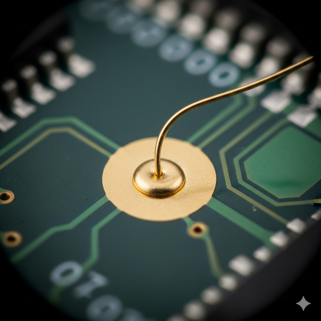
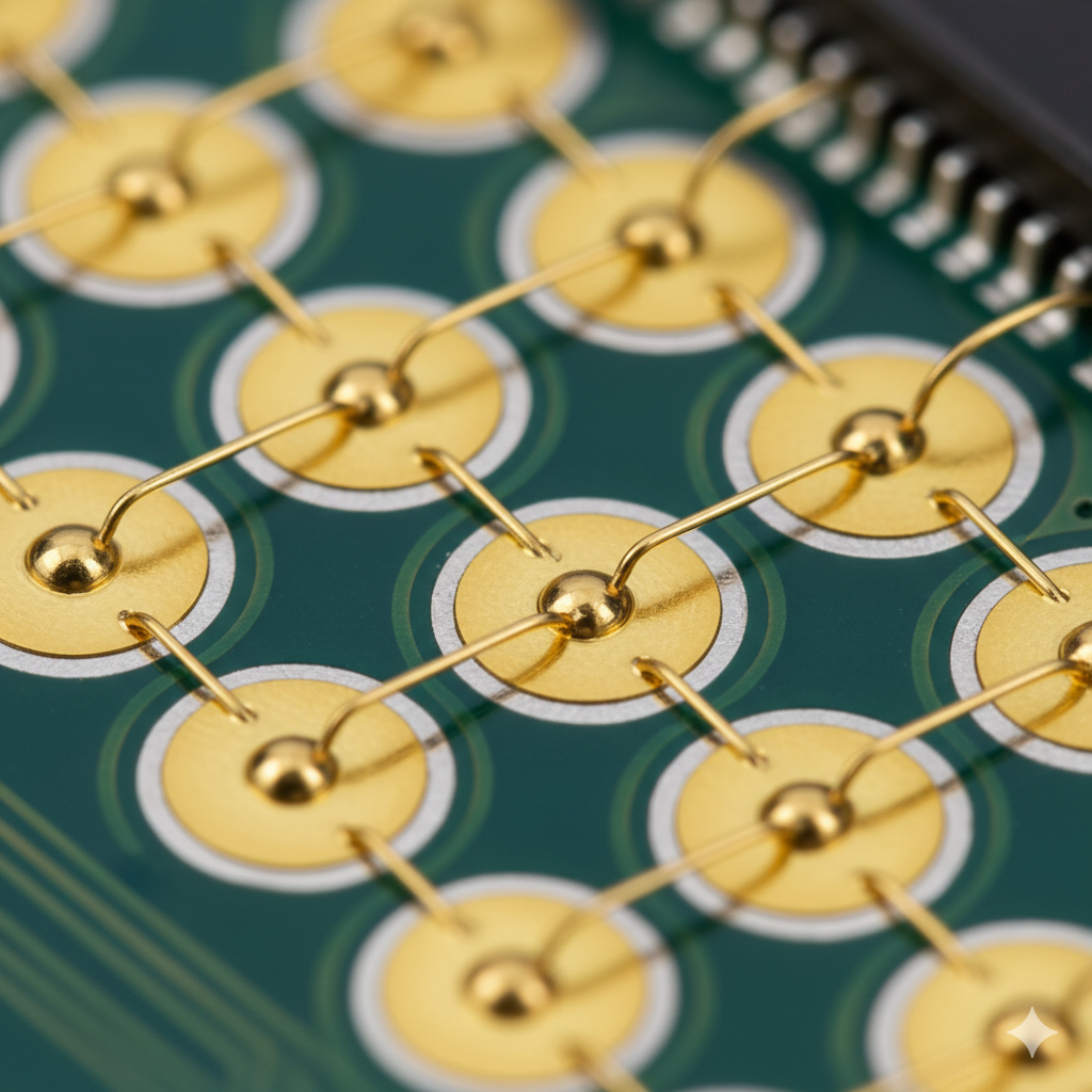
Soft gold plating is a specialized surface finish applied to printed circuit board (PCB) pads and traces, specifically designed to optimize wire bonding. This process is crucial for creating robust electrical connections between semiconductor chips and the multilayer PCB. Unlike harder gold finishes used for repeated contact points, soft gold prioritizes malleability and purity, making it ideal for the delicate operation of attaching fine wires.
The unique properties of soft gold ensure that the bond formed with wires—whether made of gold or aluminum—is both strong mechanically and highly conductive. This makes it indispensable in high-reliability applications, including aerospace, medical devices, and advanced telecommunications equipment, where connection integrity is paramount. Understanding its role helps engineers select the most appropriate surface finish for critical designs.
Why is Soft Gold Preferred for Wire Bonding Applications?
Soft gold plating stands out as a superior choice for wire bonding due to its distinct characteristics that directly contribute to connection reliability and performance. Its exceptional purity, typically 99.9% gold, ensures minimal electrical resistance at the point of connection, facilitating excellent signal transmission.
Beyond conductivity, the inherent softness of this gold layer allows for optimal deformation during the wire bonding process. This malleability enables the wire to embed effectively into the pad, forming a strong mechanical bond that resists stress and vibrations. Furthermore, soft gold significantly reduces the formation of brittle intermetallic compounds when bonded with aluminum wires, a common issue that can degrade long-term connection stability. This compatibility is vital for enduring performance, especially in environments subject to thermal cycling or mechanical strain.
How is Soft Gold Plating Applied to PCBs?
The application of soft gold plating to PCBs involves a precise, multi-step electrolytic process to achieve a uniform, bondable surface. This meticulous approach ensures the integrity and performance of the final wire bonds.
Surface Preparation and Underlayer Application
Initially, the PCB surface undergoes thorough cleaning to eliminate any contaminants, such as oils or oxides, which could compromise the adhesion of subsequent plating layers. Following this, a thin nickel underlayer is typically applied. This nickel layer acts as a crucial diffusion barrier, preventing the copper substrate from migrating into and reacting with the gold layer. This underlayer is usually between 2 to 5 micrometers thick, providing a stable foundation for the gold.
Electrolytic Gold Deposition and Quality Control
The soft gold is then deposited onto the nickel using an electrolytic process. During this stage, parameters like current density and plating time are carefully controlled to achieve a consistent thickness and uniform coverage. Additives that might harden the gold are intentionally minimized to maintain its desired softness. After plating, the surface undergoes rigorous inspection for any imperfections, such as voids or uneven thickness, which could negatively impact the subsequent wire bonding process.
What is the Optimal Soft Gold Plating Thickness for Wire Bonding?
Determining the correct thickness of the soft gold layer is a critical factor for successful wire bonding. A layer that is too thin might not provide sufficient material for a reliable bond, while an excessively thick layer can unnecessarily increase costs without proportional benefits.
Recommended Thickness Ranges for Different Wires
For most wire bonding applications, the ideal thickness for soft gold plating typically falls within a range of 0.5 to 1.5 micrometers (μm). This range strikes an optimal balance between bondability and cost-effectiveness. For gold ball wire bonding, a thickness of approximately 0.8-1.2 μm is often preferred, ensuring robust connections and excellent conductivity. When working with aluminum wedge bonding, a slightly thicker layer, usually 1.0-1.5 μm, may be more advantageous due to different bonding mechanics and the potential for intermetallic compound formation.
Avoiding Excessive Thickness
It is generally not recommended to exceed a thickness of 2.0 μm for most applications. Going beyond this can lead to issues such as gold embrittlement over time, which can compromise the long-term reliability of the bond. Collaborating closely with your online PCB manufacturer to establish the optimal thickness based on your specific wire type and bonding methodology is crucial for achieving the best possible results.
How Does Soft Gold Plating Contribute to Wire Bonding Reliability?
The long-term performance and durability of wire bonds are significantly enhanced by the properties of soft gold plating. Its characteristics directly impact the integrity of the connection under various operational conditions.
Material Purity and Environmental Stability
The high purity of soft gold minimizes the presence of contaminants at the bond interface, which are often a cause of bond failures over time. This intrinsic cleanliness ensures a more stable and reliable connection. Furthermore, soft gold exhibits excellent thermal stability, maintaining its structural integrity even through repeated temperature cycling. It can withstand temperatures up to 150°C without significant degradation, making it suitable for demanding thermal environments.
Mechanical Characteristics and Bonding Techniques
The inherent malleability of soft gold allows it to absorb mechanical stress during the bonding process. This flexibility reduces the likelihood of cracks or fractures forming in the connection, contributing to a more robust bond. To maximize this reliability, it’s essential to pair soft gold plating with appropriate bonding techniques. For example, applying the correct bonding force—typically between 20-50 grams for gold ball bonding—ensures a secure connection without causing damage to either the pad or the wire.