Introduction
In high density interconnect (HDI) PCB design, microvias enable compact routing and increased component density essential for modern electronics. The microvia aspect ratio, defined as the ratio of via depth to diameter, directly influences fabrication feasibility and long-term performance. Engineers must navigate microvia aspect ratio limits to balance interconnect density with reliability in demanding applications like smartphones and medical devices. Laser drilling for microvias has become standard due to its precision in creating small apertures. Understanding these limits ensures robust HDI structures without compromising signal integrity or mechanical strength. This article explores the principles, best practices, and reliability considerations for optimizing microvia aspect ratios.
What Is Microvia Aspect Ratio and Why It Matters
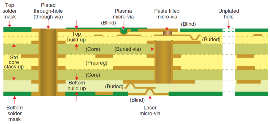
Microvia aspect ratio is calculated as the total depth of the via, including dielectric thickness and outer copper foil, divided by the via hole diameter. In HDI PCB design, microvias typically feature diameters under 150 microns and depths limited to around 100 microns to maintain feasible aspect ratios. Industry definitions, such as those in IPC-T-50M, classify microvias as blind or buried vias with maximum aspect ratios of 1:1 and depths not exceeding 0.25 mm. Exceeding these microvia aspect ratio limits risks incomplete copper plating, leading to voids or thin barrel walls that degrade electrical conductivity.
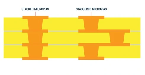
The significance of aspect ratio extends to overall board reliability, particularly in thermal cycling environments where high ratios amplify stress concentrations. In HDI structures, tight aspect ratios allow stacking or staggering microvias to achieve via-in-pad configurations, maximizing routing efficiency. Poorly managed ratios contribute to failures like via cratering or delamination, impacting microvia reliability in production-scale assemblies. Engineers prioritizing low aspect ratios enhance yield rates and extend service life in high-frequency applications.
Technical Principles of Microvia Aspect Ratio
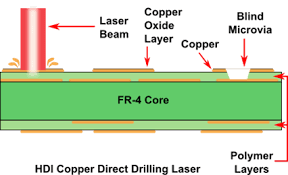
The aspect ratio governs copper electroplating uniformity during HDI fabrication, as higher ratios hinder electrolyte flow and ion deposition at the via bottom. Laser drilling for microvias produces a characteristic trumpet-shaped profile, with wider entrances and narrower bottoms, which inherently caps reliable plating at aspect ratios below 1:1. For instance, UV lasers excel at ablating dielectric materials, but excessive depth relative to diameter results in tapered walls that exacerbate plating inconsistencies. Mechanical stresses from reflow soldering further challenge high-aspect microvias, promoting microcracks under coefficient of thermal expansion mismatches.
Reliability data indicates that aspect ratios above 0.75:1 correlate with reduced cycles to failure in accelerated life tests, due to electromigration and intermetallic voiding. In stacked microvia configurations, cumulative aspect ratios across layers compound these effects, necessitating staggered alternatives for enhanced mechanical integrity. Dielectric selection influences drillability, with resin-rich materials supporting lower ratios for cleaner laser ablation. Adhering to IPC-2226 guidelines ensures these principles translate to manufacturable designs without excessive rework.
Fabrication processes like sequential lamination build HDI layers around microvias, where aspect ratio dictates fill options such as copper plating or conductive paste. Non-conductive fills demand even lower ratios to prevent resin cracks during thermal excursions. Signal propagation through microvias benefits from controlled ratios, minimizing stub effects in high-speed signals. Overall, these mechanisms underscore the need for precise ratio management from design inception.
Microvia Aspect Ratio Limits in HDI PCB Design
Microvia aspect ratio limits typically range from 0.5:1 to 1:1, with 0.75:1 serving as a practical upper bound for most production processes. In HDI PCB design, designers target minimum diameters of 75 microns paired with 50-micron dielectrics to stay within these constraints. Laser drilling for microvias enables apertures as small as 40 microns, but reliability drops sharply beyond 1:1 due to plating throw issues. Stacked vias in Type III HDI per IPC-2226 permit multiple levels, yet each must respect individual limits to avoid cumulative failures.
Environmental factors like humidity accelerate conductive anodic filamentation (CAF) in high-ratio vias, compromising insulation resistance. Thermal shock tests reveal that ratios under 0.7:1 withstand over 1000 cycles without delamination. Pad geometry, including annular ring size, interacts with aspect ratio to distribute stresses evenly. Engineers simulate these limits using stackup models to predict warpage and via performance.
Practical Solutions and Best Practices for Reliable Microvias
To achieve optimal microvia reliability, start with dielectric thicknesses under 100 microns and pair them with diameters exceeding depth by at least 25%. Laser drilling parameters should prioritize pulse energy for minimal heat-affected zones, ensuring straight sidewalls within aspect ratio limits. Post-drill desmear processes remove residue, facilitating uniform plating thicknesses of 15-20 microns. For filled microvias, select conductive epoxies compatible with low ratios to mitigate electromigration risks.
In HDI PCB design, employ design rule checks enforcing 0.8:1 maximum ratios across all microvia classes. Staggered configurations outperform stacked ones in reliability, distributing loads and reducing inter-via interactions. Qualification per IPC-6018 verifies these practices through cross-section analysis and thermal cycling. Collaborate early with fabricators to align on laser capabilities and plating chemistries.
Troubleshooting common issues involves inspecting for bottom-pad separation, often traced to ratios over 0.85:1 or inadequate cap plating. Adjust by widening diameters incrementally while monitoring impedance. For high-layer-count boards, hybrid via strategies combining microvias with filled through-holes maintain density without pushing limits.
Key Insights from HDI Microvia Implementations
Real-world HDI designs demonstrate that maintaining microvia aspect ratios below 0.75:1 yields 20-30% higher reliability margins in automotive-grade assemblies. Case analyses show staggered microvias in 12-layer stacks achieving fanout for 0.3 mm pitch BGA without signal degradation. Laser drilling advancements have pushed limits to 1:1 in select low-stress applications, but conservative ratios prevail for volume production. These insights reinforce structured approaches over aggressive density pursuits.
Conclusion
Mastering microvia aspect ratio is pivotal for advancing HDI PCB design toward higher densities and unwavering reliability. By respecting limits like 0.75:1 to 1:1, leveraging laser drilling for microvias, and following standards such as IPC-2226, engineers mitigate plating and thermal risks effectively. Practical adherence to these principles ensures robust interconnects in compact electronics. Future innovations may refine these boundaries, but current best practices provide a solid foundation for success.
FAQs
Q1: What are the standard microvia aspect ratio limits in HDI PCB design?
A1: Microvia aspect ratio limits are generally capped at 1:1 maximum, with 0.75:1 preferred for plating uniformity as outlined in IPC-2226. These ensure reliable copper deposition and minimize voids. Exceeding them risks bottom thinning and reliability failures during thermal stress. Designers calculate depth including dielectric and foil thicknesses.
Q2: How does laser drilling for microvias impact aspect ratio?
A2: Laser drilling creates trumpet-shaped holes ideal for aspect ratios up to 1:1, enabling precise small diameters in HDI structures. UV lasers ablate dielectrics cleanly, but higher ratios demand optimized pulse control to avoid taper excesses. This process supports microvia reliability by reducing mechanical stress compared to drilling. Post-processing like desmear is crucial for plating success.
Q3: Why is microvia reliability critical in high aspect ratio designs?
A3: Microvia reliability suffers at higher aspect ratios due to uneven plating and stress amplification in thermal cycling. Ratios over 0.8:1 promote cracks and CAF formation. Staggered configurations and proper fills enhance endurance. Adhering to IPC-6018 qualification tests validates performance under operational loads.
Q4: What best practices improve microvia aspect ratio management?
A4: Target 0.7:1 or lower ratios, use thin dielectrics, and verify with simulations in HDI PCB design. Prefer staggered over stacked vias for better load distribution. Laser drilling parameters must align with material properties. Early DFM reviews prevent common pitfalls like warpage.
References
IPC-2226 — Sectional Design Standard for High Density Interconnects. IPC.
IPC-6018 — Qualification and Performance Specification for High Density Interconnects. IPC.
IPC-T-50M — Terms and Definitions for Interconnecting and Packaging Electronic Circuits. IPC.


