Introduction
In the realm of printed circuit board (PCB) design, managing electromagnetic interference (EMI) is a critical challenge for electrical engineers. As electronic devices become more compact and operate at higher frequencies, the risk of EMI disrupting performance increases. Microvia design, a key element in high-density interconnect (HDI) PCBs, offers a pathway to mitigate these issues. By optimizing the structure and placement of microvias, engineers can reduce noise coupling and improve signal integrity. This article explores the principles of microvia design for EMI reduction, providing actionable insights aligned with industry standards. Aimed at professionals in electronics design, the content delves into technical mechanisms and best practices to enhance PCB performance while maintaining compliance with established guidelines.
What Are Microvias and Why Do They Matter for EMI?
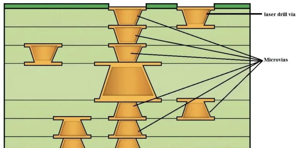
Microvias are small-diameter vias, typically less than 150 micrometers, used in HDI PCBs to connect layers in a compact space. Unlike traditional through-hole vias, microvias are often laser-drilled, allowing for precise placement in dense layouts. Their small size and ability to be stacked or staggered make them essential for modern electronics, where space constraints are common. However, their design directly impacts EMI. Poorly planned microvias can act as unintended antennas, radiating or picking up electromagnetic noise. This can degrade signal quality or interfere with nearby components. Properly implemented microvia structures minimize loop areas and reduce parasitic effects, making them a vital tool for EMI control in high-speed designs. Understanding their role is crucial for engineers aiming to balance density with performance.
Related Reading: Microvia Design for EMI Reduction
Technical Principles of EMI in PCB Design
EMI in PCBs arises from electromagnetic fields generated by current flow through traces, vias, and components. High-frequency signals create rapid changes in current, producing radiation that can couple with nearby conductors. Microvias, due to their proximity in dense layouts, can exacerbate this if not designed with care. The primary mechanisms include crosstalk, where signals interfere between adjacent vias or traces, and ground bounce, caused by inadequate return paths. Additionally, the inductance and capacitance introduced by microvias can form resonant circuits, amplifying noise at specific frequencies. Reducing these effects requires minimizing loop areas, ensuring proper grounding, and controlling impedance. Standards such as IPC-2226, which addresses HDI design, provide guidelines for via structures to limit these parasitic effects and maintain signal integrity in high-speed applications.
How Microvia Design Influences EMI
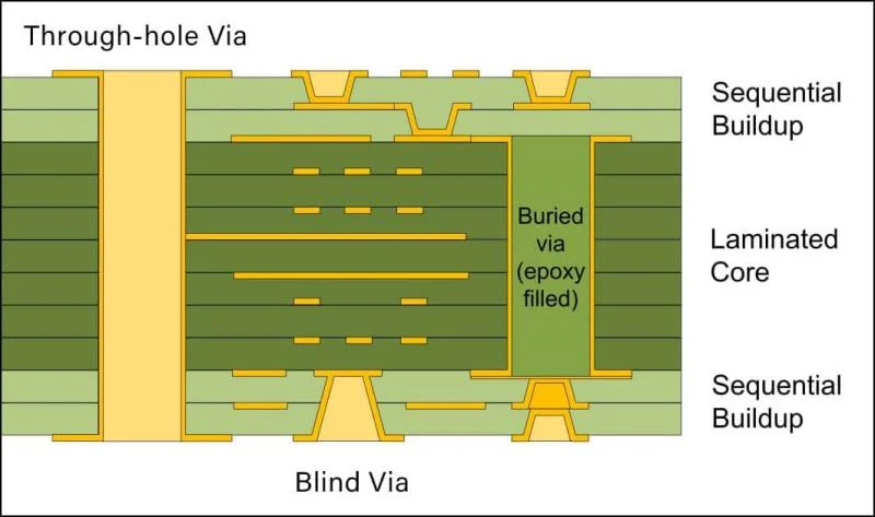
Microvia design directly affects EMI through several factors. First, the aspect ratio, or the ratio of via depth to diameter, impacts signal reflection and loss. A high aspect ratio can increase inductance, worsening EMI. Second, the placement of microvias relative to ground planes is critical. Positioning them far from a solid reference plane can create larger current loops, increasing radiated noise. Third, the type of microvia, whether blind, buried, or stacked, alters the signal path and potential interference points. Blind microvias, connecting an outer layer to an inner one, often have shorter paths, reducing loop size. Buried microvias, entirely within internal layers, can further isolate noise if paired with proper shielding. Adhering to standards like IPC-2226 helps engineers select appropriate configurations to curb EMI risks.
Practical Solutions for EMI Reduction with Microvia Design
To achieve effective EMI reduction through microvia design, engineers can adopt several strategies grounded in industry practices. These approaches focus on optimizing layout, ensuring robust grounding, and following established guidelines.
- Optimize Microvia Placement: Position microvias close to ground planes to minimize loop areas. This reduces the path length for return currents, cutting down on radiated emissions. Ensure symmetry in placement for differential pairs to avoid imbalance.
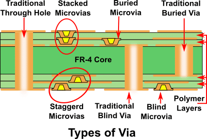
- Use Stacked or Staggered Configurations: Stacked microvias, connecting multiple layers vertically, can shorten signal paths compared to staggered designs. However, staggering can be useful to avoid thermal stress and maintain manufacturability, as outlined in IPC-2226.
- Incorporate Ground Vias: Surround critical signal microvias with ground vias to create a shielding effect. This technique, often termed a via fence, helps contain electromagnetic fields and reduce crosstalk.
- Control Aspect Ratio: Keep the aspect ratio of microvias within recommended limits, typically below 1:1 for laser-drilled vias, to minimize inductance. IPC-T-50M provides terms and definitions to guide such design choices.
- Leverage Solid Reference Planes: Ensure continuous ground and power planes beneath microvia structures. Breaks in these planes can force return currents into longer paths, increasing EMI risks.
Implementing these strategies requires balancing design density with performance. Tools for simulation can aid in predicting EMI behavior before fabrication, ensuring compliance with standards like IPC-6012E for rigid board performance.
Related Reading: Microvia PCB Design Rules: A Practical Handbook for Error Free HDI Layouts
Best Practices for Integrating Microvias in High-Speed Designs
High-speed designs amplify the challenges of EMI, making microvia integration even more critical. Start by defining clear layer stackups with dedicated ground planes adjacent to signal layers. This setup, supported by guidelines in IPC-2226, ensures minimal impedance mismatch. Next, avoid routing high-speed signals through multiple microvias unless necessary, as each transition introduces parasitic effects. When transitions are unavoidable, use back-drilling techniques to remove unused via stubs, which can act as resonant structures. Additionally, maintain consistent dielectric materials around microvias to prevent signal distortion, adhering to material selection criteria in IPC-T-50M. Finally, validate designs through signal integrity analysis to identify potential EMI hotspots. These steps collectively enhance performance while keeping electromagnetic noise in check for demanding applications.
Challenges in Microvia Design for EMI Control
While microvias offer significant benefits, they present unique challenges in EMI management. Manufacturing precision is a primary concern, as small deviations in via diameter or alignment can alter electrical characteristics. High aspect ratios, though sometimes necessary for dense designs, risk reliability issues during fabrication, potentially leading to increased inductance. Thermal expansion differences between via materials and surrounding layers can also induce stress, affecting long-term performance. Moreover, densely packed microvias in HDI layouts can create mutual coupling, where adjacent vias interfere with each other. Addressing these challenges requires strict adherence to standards like IPC-6012E, which specifies performance criteria, and thorough testing to ensure design intent translates to fabricated boards. Engineers must anticipate these issues during the design phase to avoid costly iterations.
Conclusion
Microvia design plays a pivotal role in EMI reduction for modern PCB layouts, especially in high-density and high-speed applications. By understanding the technical principles of electromagnetic interference and applying targeted design strategies, engineers can significantly enhance signal integrity and device reliability. Practical solutions, such as optimized placement, ground via shielding, and adherence to industry standards like IPC-2226 and IPC-6012E, provide a robust framework for success. While challenges in manufacturing precision and thermal management exist, careful planning and validation can mitigate risks. For electrical engineers, mastering microvia design is essential to meet the demands of compact, high-performance electronics while maintaining electromagnetic compatibility. This approach ensures that innovation in PCB design aligns with performance and compliance goals.
FAQs
Q1: How does microvia design impact EMI reduction in high-speed PCBs?
A1: Microvia design influences EMI reduction by minimizing loop areas and reducing parasitic inductance. Proper placement near ground planes and the use of shielding vias limit noise coupling. Following standards like IPC-2226 ensures optimal configurations for high-speed signals, preventing radiation and crosstalk in dense layouts.
Q2: What are key considerations for microvia placement to achieve EMI reduction?
A2: Key considerations include positioning microvias close to reference planes to shorten return paths and using ground vias for shielding. Symmetry in differential pair layouts also helps. Adhering to guidelines in IPC-2226 supports effective placement to curb electromagnetic interference.
Q3: Which industry standards guide microvia design for EMI control?
A3: Standards such as IPC-2226 for HDI design and IPC-6012E for rigid board performance are critical. IPC-T-50M offers relevant definitions and terms. These provide frameworks for via structure, aspect ratios, and layout practices to minimize EMI in PCB designs.
Q4: Why is ground plane integration vital in microvia design for EMI reduction?
A4: Ground plane integration near microvias ensures short return paths for currents, reducing loop areas that cause EMI. Continuous planes prevent ground bounce and noise coupling. Standards like IPC-2226 emphasize this practice for maintaining signal integrity in high-density designs.
References
IPC-2226 — Sectional Design Standard for High Density Interconnect (HDI) Printed Boards. IPC, 2003.
IPC-6012E — Qualification and Performance Specification for Rigid Printed Boards. IPC, 2020.
IPC-T-50M — Terms and Definitions for Interconnecting and Packaging Electronic Circuits. IPC, 2015.


