Introduction
Microvia technology has transformed the landscape of printed circuit board design, enabling high-density interconnect (HDI) layouts that support compact, high-performance electronics. For electrical engineers, mastering microvia PCB design rules is essential to ensure signal integrity, manufacturability, and reliability in modern applications like smartphones, medical devices, and automotive systems. This handbook provides a detailed exploration of HDI PCB design guidelines, focusing on critical aspects such as microvia PCB clearance, aspect ratio, and minimum drill size. By adhering to established industry standards, engineers can avoid common pitfalls and achieve error-free designs. Whether you're optimizing for space constraints or tackling complex multilayer boards, understanding these principles is key to successful implementation. Let's delve into the technical foundations and practical strategies that define effective microvia integration in HDI layouts.
What Are Microvias and Why Do They Matter in HDI Design
Microvias are small-diameter vias, typically less than 150 micrometers, used to connect layers in a printed circuit board. Unlike traditional through-hole vias, microvias are often formed using laser drilling, allowing for precise placement in HDI layouts. Their small size enables higher routing density, making them indispensable in compact designs where space is limited. In HDI PCB design guidelines, microvias facilitate the creation of multilayer boards with intricate signal paths, supporting advanced technologies like 5G and IoT devices.
The significance of microvias lies in their ability to reduce board size while maintaining functionality. They minimize signal path lengths, improving electrical performance and reducing parasitic effects. However, improper design can lead to manufacturing defects or reliability issues. Adhering to microvia PCB design rules ensures that these interconnects perform as intended, avoiding costly redesigns and ensuring compliance with industry expectations.
Technical Principles of Microvia Design in HDI Layouts
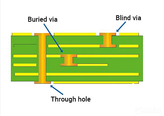
Understanding Microvia Structures and Types
Microvias come in various configurations, including blind, buried, and stacked forms. Blind microvias connect an outer layer to an inner layer, while buried microvias link internal layers without reaching the surface. Stacked microvias, often used in complex HDI designs, involve multiple microvias placed atop one another to span several layers. Each type serves a specific purpose based on the board's stack-up and routing needs.
The choice of microvia type impacts design constraints like layer count and signal integrity. According to industry standards such as IPC-2226, designers must consider the structural limitations of each configuration. For instance, stacked microvias require precise alignment to prevent mechanical stress during fabrication. Understanding these principles is fundamental to applying HDI PCB design guidelines effectively.
Related Reading: Microvia PCB for RF Applications: Design Considerations for High Frequency Performance
Key Parameters in Microvia Design
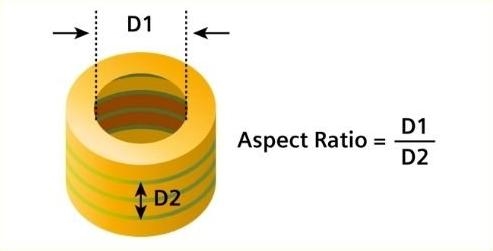
Several critical parameters define microvia performance and manufacturability. Microvia PCB aspect ratio, which is the ratio of via depth to diameter, typically should not exceed 1:1 for laser-drilled vias to ensure reliable plating and filling. Higher ratios can lead to incomplete copper deposition, risking open circuits. Standards like IPC-6012E provide specific recommendations for maintaining acceptable aspect ratios in HDI layouts.
Microvia PCB minimum drill size is another vital factor. Laser drilling often achieves diameters as small as 50 to 100 micrometers, depending on the material and equipment capabilities. However, smaller sizes increase fabrication complexity and cost. Engineers must balance design needs with practical limits, ensuring compliance with manufacturing tolerances outlined in standards such as IPC-A-600K.
Microvia PCB clearance, or the spacing between microvias and adjacent features, also plays a crucial role. Insufficient clearance can cause electrical shorts or thermal issues. Guidelines from IPC-2221B suggest minimum spacing based on voltage levels and environmental conditions to prevent breakdown or interference. These parameters collectively shape the success of an HDI design.
Challenges in Microvia Integration
Integrating microvias into HDI layouts presents unique challenges. Their small size makes them susceptible to defects like voids or cracks during plating and thermal cycling. Reliability concerns are addressed in standards such as IPC-6012E, which specify acceptance criteria for microvia structures. Thermal expansion mismatches between materials can also stress microvias, leading to failures over time.
Signal integrity is another concern, as microvias can introduce impedance discontinuities if not designed properly. High-frequency signals are particularly sensitive to such effects, necessitating careful stack-up planning. Engineers must account for these factors when applying microvia PCB design rules, ensuring that both electrical and mechanical performance are optimized.
Related Reading: Troubleshooting Microvia PCB Defects: A Guide to Identifying and Resolving Common Issues
Practical Solutions for Error-Free Microvia HDI Layouts
Adhering to Microvia PCB Design Rules
To achieve error-free HDI layouts, engineers must follow established microvia PCB design rules. Start by defining the stack-up early in the design process. This involves selecting the appropriate number of layers and microvia types to meet routing density needs. Standards like IPC-2226 offer detailed guidance on stack-up configurations for HDI boards, ensuring compatibility with manufacturing processes.
Maintain a balanced aspect ratio for microvias to facilitate reliable fabrication. As per IPC-6012E, aim for an aspect ratio of 0.75:1 or lower for optimal copper plating. This reduces the risk of defects and enhances via durability. Additionally, verify the microvia PCB minimum drill size with your fabrication partner to align with their capabilities, typically adhering to tolerances in IPC-A-600K.
Optimizing Microvia PCB Clearance
Proper spacing is critical to prevent electrical and thermal issues. Microvia PCB clearance must account for voltage ratings and environmental factors, as outlined in IPC-2221B. For high-voltage applications, increase spacing to avoid arcing or dielectric breakdown. In dense layouts, use simulation tools to identify potential interference zones and adjust clearances accordingly.
Place microvias strategically to minimize signal crosstalk. Avoid clustering them in high-density areas without adequate spacing. Following HDI PCB design guidelines, maintain uniform distribution to reduce mechanical stress during thermal cycles. Regularly consult industry standards to ensure compliance with minimum clearance requirements for your specific application.
Best Practices for Design and Verification
Incorporate design for manufacturability principles from the outset. Use microvia-friendly materials with low thermal expansion to reduce stress, as recommended in IPC-4101E for laminate specifications. Perform thorough design rule checks to catch violations of microvia PCB design rules before fabrication. This includes verifying aspect ratios, drill sizes, and clearances against standards like IPC-A-600K.
Simulate signal integrity to assess the impact of microvias on high-speed signals. Adjust via placement and stack-up to minimize reflections and delays. After design completion, conduct a pre-fabrication review to confirm alignment with HDI PCB design guidelines. This step mitigates risks and ensures a smooth transition to manufacturing.
Addressing Reliability Concerns
Reliability is paramount in HDI designs with microvias. Follow thermal management practices by distributing heat-generating components evenly across the board. Standards like IPC-6012E provide criteria for microvia integrity under thermal stress, guiding engineers in material selection and layout planning. Use filled microvias where possible to enhance structural stability.
Test prototypes under real-world conditions to identify potential failure points. Accelerated life testing, aligned with guidelines in IPC-TM-650, can reveal weaknesses in microvia structures. Document findings and refine designs to address issues, ensuring long-term performance in demanding applications.
Troubleshooting Common Microvia Design Issues
Microvia-related failures often stem from design oversights or manufacturing limitations. One frequent issue is incomplete via filling, leading to voids that compromise connectivity. This can be traced to excessive microvia PCB aspect ratio or inadequate plating processes. Refer to IPC-6012E for acceptable via fill levels and adjust design parameters accordingly.
Another common problem is microvia cracking during thermal cycles, often due to material mismatches. Select substrates and prepregs with compatible thermal properties, following specifications in IPC-4101E. If clearance violations cause shorts, revisit the layout to ensure compliance with IPC-2221B spacing rules. Systematic troubleshooting, grounded in industry standards, resolves these issues effectively.
Conclusion
Designing HDI layouts with microvias demands precision and adherence to established microvia PCB design rules. By understanding key parameters like microvia PCB aspect ratio, clearance, and minimum drill size, electrical engineers can create compact, reliable boards for cutting-edge applications. Following HDI PCB design guidelines, as outlined in recognized standards, ensures manufacturability and performance. From stack-up planning to reliability testing, each step plays a vital role in achieving error-free designs. This handbook equips professionals with the knowledge to navigate microvia challenges, paving the way for innovative and efficient PCB solutions in an increasingly connected world.
FAQs
Q1: What are the key microvia PCB design rules for ensuring reliability in HDI layouts?
A1: Reliability in HDI layouts hinges on following microvia PCB design rules like maintaining an aspect ratio below 1:1, as per IPC-6012E standards. Ensure proper clearance to avoid shorts, adhering to IPC-2221B guidelines. Use compatible materials to minimize thermal stress and verify designs with rule checks. These steps, grounded in industry standards, prevent defects and enhance board durability.
Q2: How does microvia PCB aspect ratio impact HDI design performance?
A2: Microvia PCB aspect ratio, the depth-to-diameter ratio, directly affects fabrication quality in HDI designs. Ratios exceeding 1:1 can cause incomplete plating, risking open circuits, as noted in IPC-6012E. A lower ratio, ideally 0.75:1, ensures better copper deposition and structural integrity. This balance is crucial for maintaining electrical performance and reliability.
Q3: What is the typical microvia PCB minimum drill size for HDI applications?
A3: Microvia PCB minimum drill size in HDI applications often ranges from 50 to 100 micrometers, depending on fabrication capabilities. Standards like IPC-A-600K outline acceptable tolerances for laser-drilled vias. Smaller sizes increase complexity, so engineers must confirm limits with manufacturing processes to ensure precision and avoid defects during production.
Q4: Why is microvia PCB clearance critical in high-density layouts?
A4: Microvia PCB clearance is vital to prevent electrical shorts and thermal issues in high-density layouts. Insufficient spacing can lead to arcing or interference, especially under high voltages. IPC-2221B provides spacing guidelines based on operating conditions. Proper clearance ensures signal integrity and board reliability in compact HDI designs.
References
IPC-2221B — Generic Standard on Printed Board Design. IPC, 2012.
IPC-2226 — Sectional Design Standard for High Density Interconnect (HDI) Printed Boards. IPC, 2006.
IPC-6012E — Qualification and Performance Specification for Rigid Printed Boards. IPC, 2020.
IPC-A-600K — Acceptability of Printed Boards. IPC, 2020.
IPC-4101E — Specification for Base Materials for Rigid and Multilayer Printed Boards. IPC, 2017.
IPC-TM-650 — Test Methods Manual. IPC, 2021.


