Introduction
Microvia technology has become a cornerstone in modern printed circuit board (PCB) design, especially for radio frequency (RF) applications where high-frequency performance is critical. As electronic devices push towards miniaturization and higher data rates, the demand for compact, reliable, and efficient PCB layouts intensifies. Microvias, small laser-drilled vias with diameters typically under 150 micrometers, enable high-density interconnects (HDI) essential for RF systems. These structures support intricate routing in multilayer boards while addressing challenges like signal loss and impedance matching. For electrical engineers working on RF designs, understanding how microvia PCB RF integration impacts performance is vital. This article explores key design considerations, including impedance control, signal integrity, and ground plane optimization, to ensure robust high-frequency operation in RF applications.
What Are Microvias and Why Do They Matter in RF PCB Design?
Microvias are tiny vias used in HDI PCBs to connect layers in a compact footprint. Unlike traditional through-hole vias, microvias are formed using laser drilling, allowing precise placement and smaller sizes. In RF PCB design, microvias offer several advantages. They reduce parasitic inductance and capacitance, which are detrimental to high-frequency signals. Additionally, they enable denser routing, critical for modern RF systems like 5G devices, radar modules, and satellite communication hardware. The relevance of microvia PCB RF integration lies in its ability to maintain signal integrity at gigahertz frequencies. Poorly designed microvias can introduce signal loss or impedance mismatches, leading to performance degradation. Thus, engineers must prioritize microvia design to meet the stringent demands of high-frequency applications.
Technical Principles of Microvia PCB in RF Applications
Understanding High-Frequency Challenges with Microvias
At high frequencies, RF signals are highly sensitive to physical structures within a PCB. Microvias, while beneficial for density, can act as discontinuities if not designed correctly. These discontinuities may cause reflections, leading to signal loss or distortion. The primary concerns in microvia PCB RF design include parasitic effects, where the via's geometry introduces unwanted inductance or capacitance. Additionally, the transition between layers through microvias can disrupt the electromagnetic field, affecting signal propagation. Engineers must account for these factors to minimize their impact on high-frequency performance.
Impedance Matching in Microvia PCB RF Designs
Impedance matching is a fundamental requirement for RF systems to ensure maximum power transfer and minimal reflections. In microvia PCB impedance matching RF considerations, the via's dimensions and placement play a crucial role. A mismatch can occur if the microvia alters the characteristic impedance of the transmission line. To address this, designers often use controlled impedance techniques, ensuring the microvia's aspect ratio and surrounding dielectric properties align with the trace impedance. Properly matched impedance reduces signal reflections, preserving the integrity of high-frequency signals.
Signal Loss Mechanisms in Microvia PCB RF Layouts
Signal loss in RF applications often stems from dielectric losses, conductor losses, and radiation. For microvia PCB signal loss RF challenges, the via's structure can exacerbate these issues. A poorly designed microvia may create a longer signal path, increasing conductor loss. Furthermore, if the dielectric material around the microvia has a high loss tangent, it can absorb energy from the signal. Engineers must select low-loss materials and optimize microvia placement to shorten signal paths, thereby reducing losses at high frequencies.
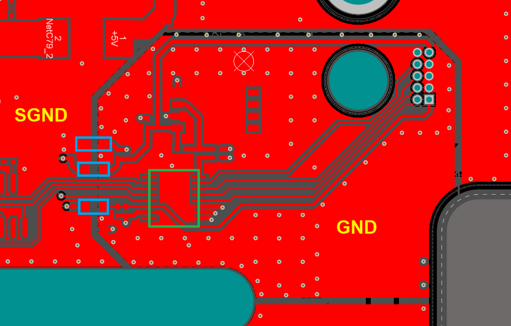
Ground Plane Interactions with Microvias in RF Designs
The ground plane is essential for providing a stable reference for RF signals. In microvia PCB ground plane RF configurations, improper via placement near the ground plane can introduce noise or crosstalk. Microvias that penetrate multiple layers may also create ground loops if not carefully integrated. A continuous, unbroken ground plane beneath critical RF traces helps maintain signal integrity by providing a low-impedance return path. Designers must ensure that microvias do not disrupt this plane, using techniques like ground via stitching to reinforce stability.
Best Practices for Designing Microvia PCB for RF Performance
Material Selection for High-Frequency Compatibility
Choosing the right substrate material is critical for microvia PCB RF designs. Materials with low dielectric constant and low loss tangent are preferred to minimize signal attenuation. Additionally, the material must support laser drilling for microvia formation without degrading. Engineers should refer to industry standards like IPC-4101C for guidance on selecting laminates suitable for high-frequency applications. Compatibility between the material and microvia process ensures reliable performance in RF systems.
Optimizing Microvia Geometry and Placement
Microvia geometry, including diameter and depth, directly impacts RF performance. Smaller diameters reduce parasitic effects, but they must be balanced with manufacturing capabilities. The aspect ratio of microvias should comply with guidelines in IPC-2226, which outlines design rules for HDI structures. Placement is equally important. Microvias should be positioned to avoid critical signal paths or areas prone to electromagnetic interference. Using simulation tools to model via behavior at high frequencies can guide optimal placement.
Ensuring Impedance Control with Microvias
To achieve microvia PCB impedance matching RF goals, designers must maintain consistent trace widths and spacing around microvias. Adding reference planes near the via can help stabilize impedance. It is also beneficial to minimize the number of layer transitions through microvias, as each transition can introduce a mismatch. Adhering to controlled impedance design practices, as specified in IPC-2141A, ensures reliable signal transmission in RF applications.
Minimizing Signal Loss through Design Techniques
Reducing microvia PCB signal loss RF issues requires careful attention to signal routing. Avoid sharp bends in traces near microvias, as these can cause reflections. Additionally, using shorter microvias by limiting stack-up height can decrease conductor loss. Designers should also place ground vias strategically around signal microvias to shield against crosstalk. Following best practices in trace design, as outlined in IPC-2251, helps maintain signal integrity at high frequencies.
Ground Plane Design for RF Stability
For microvia PCB ground plane RF optimization, a solid ground plane is indispensable. Ensure that microvias do not fragment the ground plane, especially under high-frequency traces. Stitching vias can be used to connect ground planes across layers, maintaining a low-impedance path. Additionally, keep sensitive RF components close to the ground plane to reduce noise pickup. Guidelines from IPC-2221B provide detailed recommendations for ground plane design in multilayer PCBs.
Practical Insights for RF PCB Design with Microvias
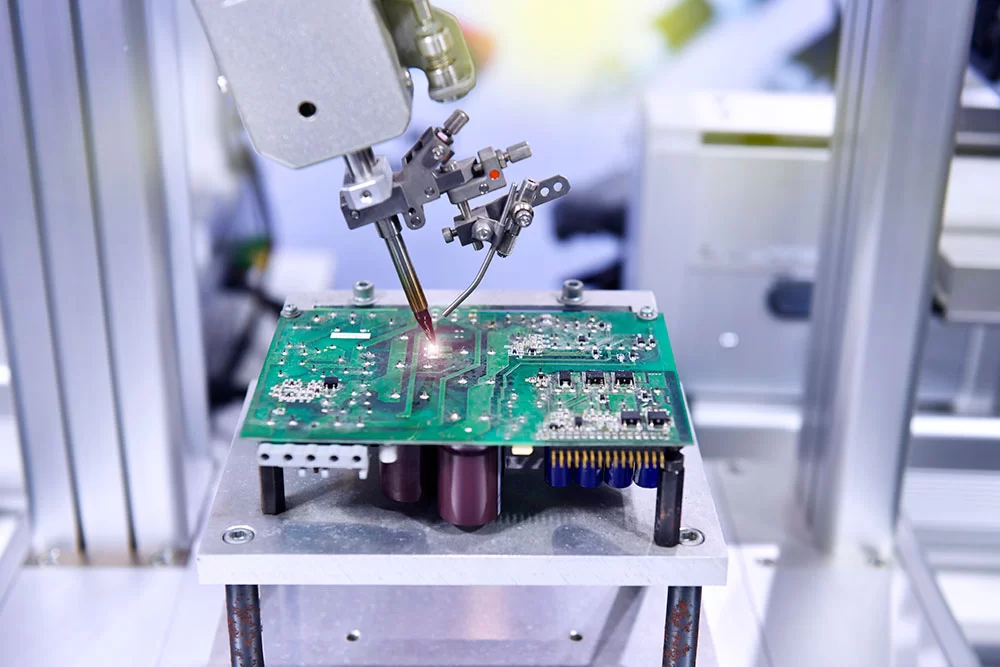
Designing microvia PCB RF layouts often involves balancing performance with manufacturability. One common challenge is ensuring reliable microvia formation without defects like voids or cracks, which can degrade high-frequency signals. Engineers should collaborate closely with fabrication teams to verify that microvia drilling and plating processes meet standards like IPC-6012E. Another insight is the use of back-drilling for unused via stubs, which can act as resonators at high frequencies. While this adds complexity, it significantly reduces signal reflections. Simulation prior to fabrication is also recommended to predict how microvias affect impedance and signal loss, allowing adjustments before costly prototyping.
Conclusion
Microvia technology offers immense potential for RF PCB design, enabling high-density layouts essential for modern high-frequency applications. However, achieving optimal performance requires meticulous attention to design considerations like impedance matching, signal loss mitigation, and ground plane integrity. By selecting appropriate materials, optimizing microvia geometry, and adhering to industry standards, engineers can overcome the challenges of microvia PCB RF integration. These practices ensure reliable operation in demanding environments like telecommunications and aerospace. With careful planning and simulation, microvia PCB designs can meet the stringent requirements of high-frequency systems, paving the way for innovative electronic solutions.
FAQs
Q1: How do microvias impact impedance matching in microvia PCB RF designs?
A1: Microvias can disrupt impedance if their geometry or placement alters the characteristic impedance of RF traces. To ensure microvia PCB impedance matching RF performance, maintain consistent trace dimensions and use reference planes. Following standards like IPC-2141A helps achieve controlled impedance. Simulation tools can also predict and mitigate mismatches before fabrication.
Q2: What causes signal loss in microvia PCB RF applications?
A2: Signal loss in microvia PCB signal loss RF scenarios arises from dielectric absorption, conductor resistance, and reflections at via transitions. Poorly designed microvias extend signal paths, increasing loss. Using low-loss materials and optimizing via placement, as per IPC-2251 guidelines, reduces these effects and preserves high-frequency signal integrity.
Q3: Why is the ground plane critical for microvia PCB ground plane RF performance?
A3: The ground plane provides a stable reference for RF signals, minimizing noise and crosstalk. In microvia PCB ground plane RF designs, disruptions from vias can create ground loops. Stitching vias and maintaining plane continuity, per IPC-2221B, ensure a low-impedance return path, enhancing signal stability in high-frequency systems.
Q4: How can engineers optimize microvia placement in RF PCB design microvias?
A4: Optimizing microvia placement in RF PCB design microvias involves avoiding critical signal paths and minimizing layer transitions. Keep microvias away from high-frequency traces to reduce interference. Adhering to IPC-2226 design rules for HDI structures and using simulation for placement validation ensures performance without compromising manufacturability.
References
IPC-6012E — Qualification and Performance Specification for Rigid Printed Boards. IPC, 2020.
IPC-2226 — Sectional Design Standard for High Density Interconnect (HDI) Printed Boards. IPC, 2003.
IPC-2141A — Design Guide for High-Speed Controlled Impedance Circuit Boards. IPC, 2004.
IPC-2251 — Design Guide for the Packaging of High Speed Electronic Circuits. IPC, 2003.
IPC-2221B — Generic Standard on Printed Board Design. IPC, 2012.
IPC-4101C — Specification for Base Materials for Rigid and Multilayer Printed Boards. IPC, 2009.


