Introduction
Electric vehicle battery management systems rely on printed circuit boards to monitor cell voltages, temperatures, and currents while ensuring safe operation under harsh electromagnetic environments. These PCBs face significant electromagnetic interference challenges from high-power switching converters, inverter drives, and nearby high-voltage bus bars. Minimizing EMI through effective shielding and layout practices is crucial for maintaining signal integrity and passing regulatory compliance. Poor EMI control can lead to false readings, communication errors, or system failures in EVs. This article explores proven strategies tailored for EV BMS PCBs, focusing on ground plane design, filtering techniques, and testing protocols. Engineers can implement these methods to enhance reliability without compromising performance.
Electromagnetic interference in EV BMS PCBs arises from both internal sources like PWM signals from DC-DC converters and external fields from the vehicle's powertrain. Radiated EMI couples through traces acting as antennas, while conducted EMI travels via power lines and ground returns. In battery packs, rapid current changes in cell balancing circuits generate noise that propagates across layers. Signal integrity suffers when high-frequency harmonics distort analog sensor data or digital protocols like CAN bus. Compliance with automotive EMC requirements demands proactive design to suppress emissions below limits. Addressing EMI early prevents costly redesigns and ensures robust operation in dense EV electronics.
Understanding EMI in EV Battery Management PCBs
EV BMS PCBs operate in environments with strong magnetic fields from battery currents exceeding hundreds of amps, amplifying susceptibility issues. Common failure modes include voltage measurement inaccuracies due to crosstalk or reset glitches in microcontrollers from coupled noise. Ground loops exacerbate differential mode noise, turning benign signals into interference sources. Layout choices directly influence impedance mismatches that reflect waves and increase emissions. Understanding these mechanisms allows engineers to prioritize shielding and partitioning from the schematic stage.
Key Technical Principles of EMI Generation and Coupling
EMI generation follows Faraday's law, where changing magnetic fields induce voltages in loops formed by PCB traces. In EV BMS, fast edges from MOSFET switching create broadband spectra up to hundreds of MHz. Coupling occurs capacitively between adjacent traces or inductively via mutual inductance in parallel runs. Common-mode currents on cables radiate efficiently if not balanced. Signal integrity degrades through reflections at impedance discontinuities, causing overshoot and ringing that radiate further. Ground plane design plays a pivotal role by providing low-impedance return paths, reducing loop areas that act as antennas.
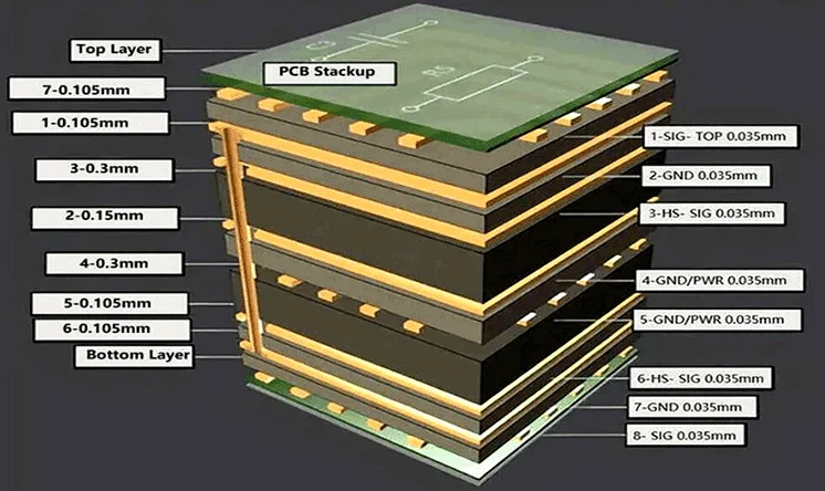
Differential signaling mitigates EMI by canceling common-mode components, ideal for sensor interfaces in BMS. However, imbalance in pair lengths introduces conversions to common mode. Filter design targets specific frequencies, with pi-networks attenuating harmonics from clock oscillators. Common mode chokes block symmetric noise on twisted pairs or power lines without affecting differential signals. Layer stackup influences field containment, with ground planes sandwiching signal layers to shield E-fields. Adhering to IPC-2221 guidelines for trace spacing and via placement minimizes unintended coupling paths.
Best Practices for Ground Plane Design
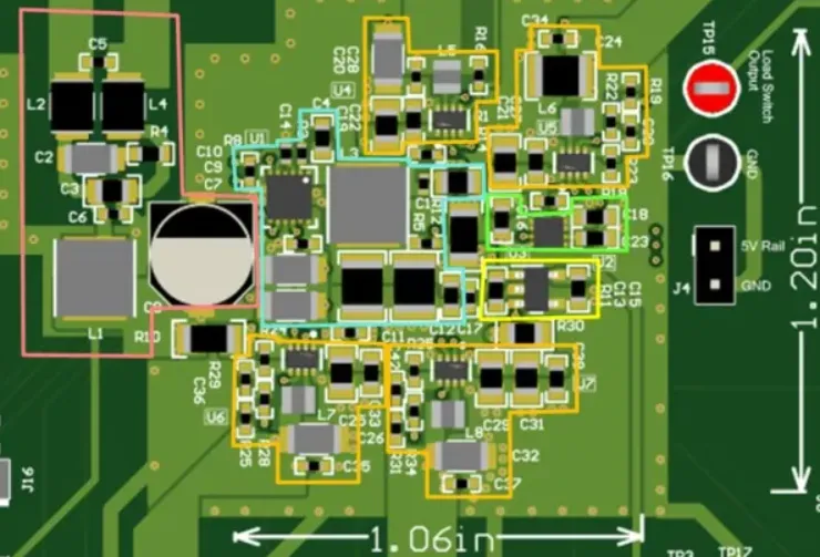
A continuous ground plane across inner layers forms the foundation of EMI shielding PCB strategies in EV BMS designs. Split planes only at isolated analog-digital boundaries, stitching with dense vias to prevent slots that radiate. Place ground planes adjacent to signal layers to shorten return currents and confine fields. In multi-layer boards, dedicate full layers to ground rather than fragmented pours, ensuring uniform potential. This approach maintains signal integrity by stabilizing reference impedances for high-speed traces. Engineers should simulate plane resonance to avoid quarter-wave modes aligning with switching frequencies.
Via stitching around cutouts and edges creates a Faraday cage effect, shunting high-frequency currents. Connect multiple ground vias under ICs to spread return paths, reducing inductance. For EV BMS, separate chassis ground from signal ground at a single point near the connector to break loops. Power planes should overlap ground minimally, with decoupling capacitors bridging them. These practices align with structured layer sequencing, such as signal-ground-signal-ground for optimal isolation.
Enhancing Signal Integrity Through Routing and Shielding
Route critical signals like current shunts as differential pairs with matched lengths and tight coupling to reject noise. Guard traces flanked by grounded lines shield sensitive analog paths from digital aggressors. Keep high-speed traces short and away from board edges to minimize antenna effects. For EMI shielding PCB effectiveness, apply copper pours over sensitive areas, connected via stitching vias every few millimeters. Enclose noisy sections like gate drivers under metal cans grounded to the plane. These techniques preserve signal integrity amid the high di/dt environments of EV batteries.
Impedance control at 100 ohms for differential pairs ensures minimal reflections, critical for CAN and LIN communications in BMS. Avoid right-angle bends, opting for 45-degree mitered corners to reduce radiation. Power routing uses wide traces or planes to lower resistance, preventing voltage droop that induces noise. Shielding effectiveness improves with via fences around connectors, forming labyrinthine barriers for E-fields.
Filter Design and Component Selection for EMI Suppression
Filter design in EV BMS PCBs starts with placement near noise entry points, such as power inputs from the battery pack. Ferrite beads on DC lines absorb high-frequency common-mode noise, complementing bypass capacitors. Pi-filters with series inductors and shunt capacitors provide broadband attenuation for conducted EMI. Common mode chokes excel at suppressing symmetric currents on sensor cables without degrading differential signaling. Select components rated for automotive temperatures and vibrations to ensure longevity.
Tailor cutoff frequencies to target switching harmonics, typically 100 kHz to 10 MHz in BMS converters. Layout capacitors close to IC pins with short, wide traces to minimize ESL. For signal integrity, add RC snubbers across switching nodes to dampen ringing. These elements form a robust defense, reducing emissions to pass pre-compliance scans.
Integrating Differential Signaling and Layout Partitioning
Differential signaling inherently rejects common-mode EMI, making it suitable for voltage sensing across battery cells. Maintain pair symmetry with ground reference planes beneath for balanced fields. Partition the board into zones: power, analog, digital, with moats separating them. Route clocks and clocks internally, away from edges. This zoning preserves signal integrity while localizing noise.
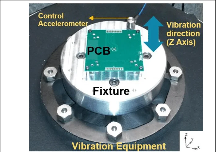
EMC Testing Essentials for Validation
EMC testing verifies EMI shielding PCB performance through radiated and conducted measurements in anechoic chambers. Conduct pre-compliance scans early to iterate layouts. Immunity tests per IEC 61000 expose boards to ESD, surges, and fields simulating EV conditions. Optimize based on failure margins, adjusting ground plane design or adding filters. Full certification confirms compliance for vehicle integration. Iterative testing refines signal integrity without over-engineering.
Conclusion
Effective EMI minimization in EV battery management PCBs demands integrated shielding and layout best practices from ground plane design to filter design. Prioritizing continuous planes, differential signaling, and common mode chokes ensures signal integrity amid aggressive noise. EMC testing validates these efforts, aligning with standards like IPC-2221 and IEC 61000. Engineers adopting these strategies achieve reliable BMS performance, supporting safer EVs. Proactive design reduces risks, accelerates development, and meets stringent automotive demands.
FAQs
Q1: What role does ground plane design play in EMI shielding PCB for EV BMS?
A1: Ground plane design provides low-impedance return paths, minimizing loop areas that radiate EMI. Solid planes adjacent to signals confine fields and enhance signal integrity. Stitching vias prevent slots acting as antennas. This foundation supports filter design and shielding effectiveness in high-noise EV environments.
Q2: How does differential signaling improve signal integrity in battery management PCBs?
A2: Differential signaling cancels common-mode noise, ideal for precise cell monitoring. Matched pairs with controlled impedance reject interference from switching converters. Ground planes beneath balance the fields, reducing crosstalk. Combined with guard traces, it maintains data accuracy during EMC testing.
Q3: Why use common mode chokes in EMI mitigation for EV PCBs?
A3: Common mode chokes block symmetric noise on power lines and cables without affecting differential signals. Placed near connectors, they suppress conducted EMI from battery currents. Paired with capacitors, they form effective filters targeting EV harmonics. This preserves overall signal integrity.
Q4: What are key steps in EMC testing for EV battery PCBs?
A4: EMC testing involves emissions scans for radiated and conducted noise, plus immunity to fields and surges per IEC 61000. Pre-compliance identifies issues like poor ground plane design early. Iterate layouts, adding shielding or filters as needed. Final validation ensures automotive compliance.
References
IPC-2221 — Generic Standard on Printed Board Design. IPC, 2003
IEC 61000-6-3 — Electromagnetic compatibility (EMC) - Part 6-3: Generic standards - Emission standard for residential, commercial and light-industrial environments. IEC, 2020