Introduction
High-current PCB designs present unique challenges in managing heat dissipation, where excessive temperatures can degrade component performance and reduce overall system reliability. Electrical engineers often rely on thermal vias and via stitching to transfer heat from power traces and components to inner layers or heat sinks effectively. The minimum drill size for these vias plays a critical role, as it influences plating thickness, thermal conductance, and manufacturing feasibility. Balancing smaller drills for density with larger ones for better heat transfer defines successful thermal management PCB strategies. This article explores the principles behind pcb drill size thermal vias, practical guidelines for high current pcb design, and best practices for via stitching thermal applications. Understanding these elements ensures compliance with industry standards and optimal heat dissipation pcb performance.
Understanding Minimum Drill Size in High-Current PCBs
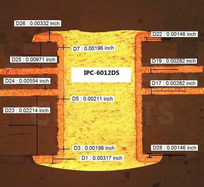
The minimum drill size refers to the smallest hole diameter that PCB fabricators can reliably produce while maintaining plating integrity and aspect ratios. For standard vias, IPC-6012 specifies a minimum of 150 microns (6 mils) for via-in-pad designs in Class 3 assemblies, accounting for drill wander and plating tolerances. In high-current applications, thermal vias demand careful sizing to maximize cross-sectional area for heat flow without compromising board density. Smaller drills limit copper plating thickness, increasing thermal resistance, while larger drills enhance conductivity but occupy more space under components. Engineers must consider board thickness, typically keeping aspect ratios below 10:1 to avoid plating voids. This parameter directly impacts heat dissipation pcb efficiency, as via arrays under power devices like QFNs or transistors form vertical heat paths to ground planes.
Why does minimum drill size matter for thermal management pcb? Inadequate sizing leads to hotspots, accelerating electromigration in traces and delamination in multilayers. High current pcb design requires vias that not only carry electrical current but also dissipate joule heating effectively. Industry guidelines from IPC-2221 emphasize via dimensions compatible with stackup and thermal predictions, preventing failures in demanding environments. Selecting the right size optimizes the trade-off between thermal performance and routability, especially in dense layouts with multiple power rails.
Technical Principles of Thermal Vias and Drill Size
Thermal conduction through vias follows principles where heat transfer rate Q equals delta T over thermal resistance R_th, with R_th inversely proportional to via diameter squared due to area A = π (d/2)^2. Larger drill sizes yield thicker plating, reducing R_th and improving heat dissipation pcb from sources like wide power traces. Plated copper walls provide the primary path, but air gaps or thin plating in small drills elevate resistance significantly. Filling vias with conductive epoxy further lowers R_th by replacing low-conductivity air, making it essential for high-power applications. Aspect ratio constraints ensure uniform plating; for a 1.6 mm thick board, drills below 0.16 mm risk incomplete coverage.
Via stitching thermal involves arrays of vias connecting traces across layers, distributing current and heat loads. Each via shares the burden, preventing overload on individuals, while collective area boosts plane spreading. Spacing influences effectiveness: closer pitches enhance conduction but risk crosstalk or mechanical stress. IPC-2152 guidelines aid in predicting trace temperatures, incorporating via contributions to overall thermal models. In multilayers, stitching to inner planes leverages copper's high in-plane conductivity for lateral dissipation.
For pcb drill size thermal vias, typical ranges start at 0.2 mm to 0.4 mm (8 to 16 mils), balancing conductance with density under pads. Smaller 0.25 mm vias suit fine-pitch components, while 0.3 mm offers optimal plating for moderate currents. Engineers simulate arrays to quantify reductions in peak temperatures, often achieving 20-30% improvements with filled patterns.
Practical Solutions and Best Practices for Thermal Management
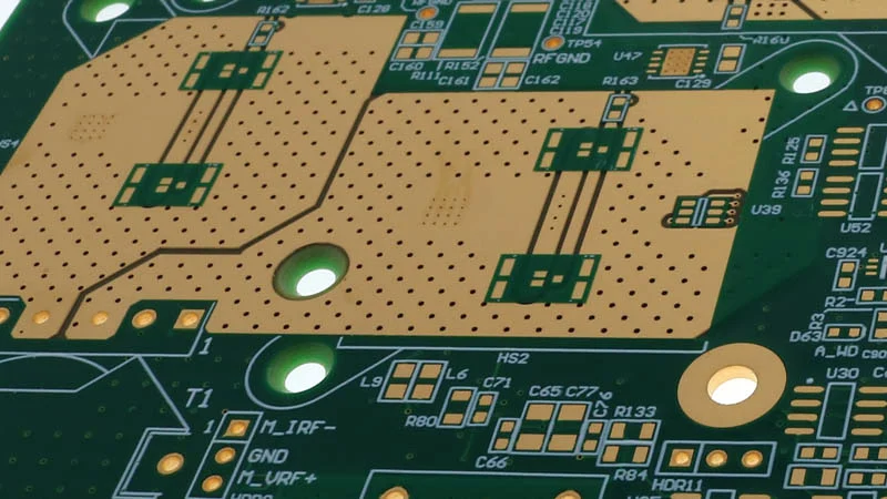
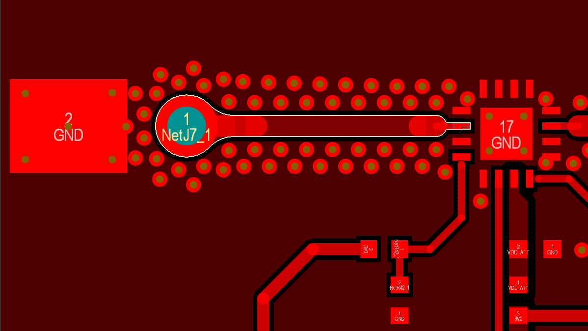
Start with component thermal pads: place via arrays directly beneath, using grid patterns with 1 to 1.2 mm center-to-center spacing to minimize lateral losses. Density of 10 to 50 vias per cm2 scales with power, connected in parallel to ground planes for low-inductance paths. Avoid thermal reliefs on these vias, as they impede flow; instead, use solid connections. For high current pcb design, select drill sizes per IPC-2222 levels, adding 0.20 to 0.25 mm to lead diameters for reliable holes.
Via stitching along traces requires placement every few millimeters, numerous small vias preferred over few large ones to match trace impedance. Distribute evenly to avoid hotspots, combining with wide pours for hybrid conduction. In power distribution, stitching doubles layer capacity by linking top and internal traces. Validate with fabricators early, confirming drill capabilities and stackup effects on warpage.
Thermal Via (Single) — Recommended Drill Diameter: 0.25-0.3 mm — Typical Use Case: Under IC pads — Key Consideration: Filling for low R_th
Stitching Via — Recommended Drill Diameter: 0.2-0.4 mm — Typical Use Case: Along power traces — Key Consideration: Spacing λ/20 for RF
High-Current Array — Recommended Drill Diameter: 0.3-0.5 mm — Typical Use Case: Multi-layer heat paths — Key Consideration: Aspect ratio <10:1
Additional strategies include thicker copper (2 oz+), copper pours, and simulation per IPC-2152 for current limits. Prototype testing confirms models, adjusting densities for real-world dissipation.
Common Pitfalls and Troubleshooting in Via Implementation
Engineers often undersize thermal vias, leading to insufficient plating and high R_th under high loads. Clustering vias near edges causes warpage; stagger across layers instead. Solder wicking in unfilled vias during assembly disrupts joints, resolved by tenting or filling. In high current pcb design, ignoring via current derating per IPC-2152 results in trace fusing; model each via's share.
Troubleshoot hotspots with IR imaging post-assembly, adding stitching if planes saturate. Mechanical stress from dense arrays demands reinforced pads per IPC-6012 annular ring rules (2 mils external Class 3). Collaborate on DFM to align drill sizes with fab limits.
Conclusion
Optimizing minimum drill size for thermal vias and via stitching forms the cornerstone of effective thermal management pcb in high-current designs. From 0.2 mm drills for density to arrays enhancing conductance, these strategies ensure reliable heat dissipation pcb while adhering to IPC guidelines. Engineers achieve lower temperatures, extended lifespans, and compliance through structured sizing, patterns, and validation. Prioritizing these principles elevates high current pcb design from functional to robust.
FAQs
Q1: What is the minimum pcb drill size thermal vias for high-current applications?
A1: Typical minimums start at 0.15 mm (6 mils) per IPC-6012 for Class 3, but 0.2-0.4 mm drills are recommended for thermal vias to ensure thick plating and low resistance. Larger sizes improve heat transfer in power components, balanced against density. Always verify aspect ratios below 10:1 with fabricators.
Q2: How does via stitching thermal improve high current pcb design?
A2: Via stitching connects traces to planes, sharing current and spreading heat across layers for better thermal management pcb. Use numerous 0.2-0.4 mm vias spaced evenly along paths to prevent hotspots. This doubles capacity in multilayers and aids dissipation without large singles.
Q3: What factors determine pcb drill size thermal vias selection?
A3: Board thickness, power density, and plating needs dictate sizes, with 0.25-0.3 mm common for efficiency. IPC-2221 guides compatibility, while simulations per IPC-2152 predict performance. Filling enhances conductance for heat dissipation pcb under demanding loads.
Q4: Why fill thermal vias in high-current PCBs?
A4: Conductive fills replace air, slashing thermal resistance and preventing wicking during soldering. Essential for arrays under pads, they boost vertical conduction in thermal management pcb strategies.
References
IPC-6012 — Qualification and Performance Specification for Rigid Printed Boards. IPC
IPC-2221 — Generic Standard on Printed Board Design. IPC
IPC-2152 — Standard for Determining Current Carrying Capacity in Printed Board Design. IPC


