What Role Does Dielectric Thickness Play in Multilayer PCBs?
When designing a multilayer Printed Circuit Board (PCB), the dielectric thickness—the insulating material separating conductive layers—is a crucial element. This seemingly minor detail profoundly influences signal integrity, power distribution efficiency, and the minimization of electrical interference. Optimizing this thickness involves balancing factors like impedance control, signal propagation speed, and effective power plane design, alongside careful material selection and layer arrangement.
Dielectric thickness refers to the precise distance between conductive elements, such as signal traces or power planes, within a multilayer PCB. These layers are insulated by dielectric materials, commonly FR-4 (a fiberglass-epoxy laminate) or more specialized materials with distinct electrical properties. This thickness directly affects how electrical signals propagate, the extent of crosstalk between adjacent traces, and the efficiency of power distribution across the board. In typical multilayer stackups (e.g., 4, 6, 8, or more layers), dielectric thickness varies based on specific design objectives. For instance, a thinner dielectric layer might be used between a signal layer and a ground plane to precisely control impedance, whereas a thicker dielectric could be chosen between power and ground planes to manage capacitance. Understanding and fine-tuning this thickness is paramount for achieving high performance in intricate electronic designs.

Why is Dielectric Thickness Critical for Multilayer PCB Stackup?
The dielectric thickness within a multilayer PCB stackup extends beyond mere physical separation; it fundamentally impacts electrical performance. Here's why its optimization is so important:
Signal Integrity and Impedance Control
Dielectric thickness directly influences the characteristic impedance of signal traces. For high-speed designs, maintaining consistent impedance (often 50 ohms for single-ended signals) is essential to prevent signal reflections and data loss. A thinner dielectric between a signal layer and its reference plane (typically ground) decreases impedance, while a thicker dielectric increases it.
Crosstalk, EMI, and Power Plane Dynamics
Thinner dielectric layers can elevate the risk of crosstalk between adjacent signal traces or layers. Appropriate dielectric thickness helps isolate signals and mitigate electromagnetic interference (EMI). In power distribution networks, the dielectric thickness between power and ground planes dictates capacitance. A thinner dielectric increases capacitance, which can aid in noise filtering but may also lead to unwanted coupling if not managed carefully.
Impact on Signal Speed
Both the dielectric constant (Dk) of the material and its thickness influence signal propagation delay. A lower Dk and an optimized thickness can facilitate faster signal travel, a critical factor for high-frequency applications. By meticulously selecting dielectric thickness, you can fine-tune your PCB layer arrangement to meet the specific demands of your application, whether it involves high-speed digital circuits or power-intensive designs.
What Factors Influence Dielectric Layer Thickness Selection?
Optimizing the dielectric layer thickness in a multilayer PCB stackup demands a careful consideration of multiple interacting factors. Understanding these elements is key to making informed design choices.
Impedance Control for Signal Quality
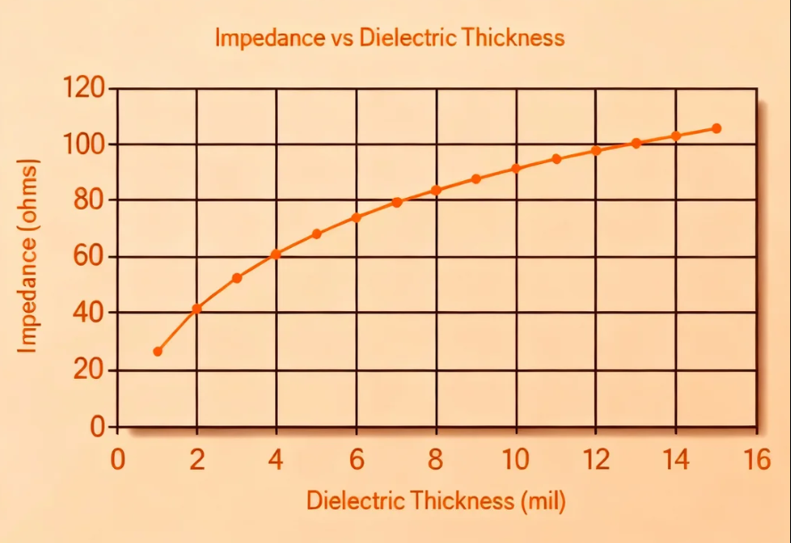
For signals operating at high speeds, precise impedance control is essential. The dielectric thickness situated between a signal trace and its accompanying reference plane (typically a ground plane) directly impacts this. A general guideline involves selecting a dielectric thickness that yields the target impedance, based on the trace width and the material’s dielectric constant. For instance, with standard FR-4 (Dk around 4.2-4.5), a 0.127 mm (5-mil) dielectric thickness might be chosen to achieve 50-ohm impedance when using a 0.178 mm (7-mil) wide trace. Most modern design software includes simulation tools to assist in calculating and verifying these values.
Layer Count and Overall Board Dimensions
The total number of layers in a multilayer PCB stackup also dictates dielectric thickness choices. A 6-layer board, for example, might feature thinner dielectrics compared to a 12-layer board to maintain a manageable overall board thickness (typically 1.6 mm for standard designs). However, excessively compressing many layers into a thin board can lead to manufacturing difficulties and compromised signal performance. Close collaboration with your PCB fabrication team is crucial to ensure dielectric thicknesses align with both design specifications and production capabilities.
Capacitance in Power Plane Design
In the context of power distribution, the dielectric thickness between power and ground layers directly affects interplane capacitance. A thinner dielectric (e.g., 0.076-0.127 mm or 3-5 mils) increases capacitance, which can act as a natural decoupling capacitor to suppress noise. Conversely, an overly thin dielectric might lead to excessive coupling or manufacturing defects like short circuits. For high-voltage designs, a thicker dielectric (e.g., 0.254-0.508 mm or 10-20 mils) may be preferable to prevent electrical breakdown.
Material Properties
The characteristics of the dielectric material, such as its dielectric constant (Dk) and dissipation factor (Df), interact with thickness to influence overall performance. Materials with a lower Dk (e.g., some advanced laminates) enable faster signal propagation and may necessitate different thickness selections compared to conventional FR-4. Always consult the material specifications when planning your stackup.
Best Practices for Optimizing Dielectric Thickness in PCB Stackup
Once the importance of dielectric thickness is understood, implementing best practices for its optimization in your multilayer PCB stackup is crucial for maximizing performance.
Strategic Early Stackup Planning
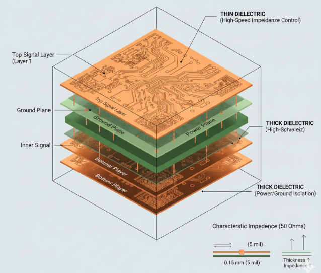
Begin by clearly defining the function of each layer within your PCB arrangement. For instance, in a 6 layer pcb stackup, a typical configuration might involve:
● Layer 1: Top Signal
● Layer 2: Ground Plane
● Layer 3: Inner Signal
● Layer 4: Inner Signal
● Layer 5: Power Plane
● Layer 6: Bottom Signal
Strategically place ground planes adjacent to signal layers using thin dielectrics (e.g., 0.1-0.15 mm or 4-6 mils) to preserve signal integrity in multilayer designs. Position power and ground planes next to each other with a dielectric thickness that balances capacitance and isolation (e.g., 0.254 mm or 10 mils).
Leveraging Simulation Tools
Modern PCB design software often includes built-in stackup editors and impedance calculators. Utilize these tools to experiment with different dielectric thicknesses and materials before finalizing your design. For example, simulating a 50-ohm trace with a 0.127 mm (5-mil) dielectric might show a perfect impedance match, whereas a 0.254 mm (10-mil) dielectric could push the impedance to 75 ohms, leading to signal mismatches.
Crosstalk Reduction Through Spacing
Avoid placing high-speed signal layers in close proximity to each other without an intervening ground plane. A dielectric thickness of at least 0.2-0.254 mm (8-10 mils) between signal layers can significantly reduce crosstalk, particularly in densely packed designs. If space is limited, prioritize thinner dielectrics only in areas where stringent impedance control is absolutely essential.
Collaborative Manufacturing Approach
Not all dielectric thicknesses are equally easy or cost-effective to fabricate. Standard thicknesses like 0.127 mm (5 mils), 0.254 mm (10 mils), or 0.508 mm (20 mils) are typically readily available, but custom values may increase costs or lead times. Early engagement with your fabrication partner ensures your multilayer PCB stackup design is manufacturable without compromising performance goals.
Iterative Testing and Refinement
Following the prototyping phase, thoroughly test your PCB for signal integrity, power stability, and electromagnetic interference. Instruments such as oscilloscopes and network analyzers can reveal if dielectric thickness choices are contributing to issues like signal reflections or unwanted noise. Adjust your stackup design in subsequent iterations as necessary to address any identified problems.
Overcoming Common Hurdles in Dielectric Thickness Optimization
Despite meticulous planning, challenges can still emerge during the optimization of dielectric thickness. Here are frequent issues and their corresponding solutions:
● Manufacturing Limitations: Extremely thin dielectrics (below 0.076 mm or 3 mils) can be difficult to fabricate consistently. Solution: Adhere to standard thicknesses or opt for prepreg materials known to provide reliable thin layers.
● Signal Reflections: Incorrect dielectric thickness is a primary cause of impedance mismatches. Solution: Implement controlled impedance design principles and rigorously verify with simulations.
● Cost Implications: Advanced dielectric materials or non-standard thicknesses can lead to increased costs. Solution: Balance performance requirements with budget constraints by using standard FR-4 materials in areas where ultra-high performance is not critical.
● Thermal Concerns: Thin dielectrics in power plane designs can contribute to localized heat buildup. Solution: Increase dielectric thickness in high-current zones or enhance thermal management through vias and heat sinks.
Dielectric Thickness Considerations for High-Speed and High-Power Designs
Different electronic applications present unique requirements for dielectric thickness. Let's explore two common design scenarios:
High-Speed Digital Applications
For interfaces such as USB, HDMI, or DDR memory, signal integrity in multilayer PCBs is paramount. The dielectric thickness between signal and ground layers should be minimized (e.g., 0.076-0.127 mm or 3-5 mils) to maintain tight impedance control. Furthermore, utilizing low-loss dielectric materials with a Dk below 3.5, if feasible, can significantly reduce signal delay.
High-Power Circuitry
In power electronics, including motor drives or power supplies, the focus shifts to the dielectric thickness between power and ground planes. A thickness of 0.254-0.508 mm (10-20 mils) often provides sufficient isolation while still offering some inherent capacitance for noise reduction. It is critical to ensure the chosen material can withstand high voltages without breakdown; always verify the dielectric strength rating (typically 20-50 kV/mm for pcb FR4 material).
Mastering Dielectric Thickness for Optimal PCB Performance
Dielectric thickness in multilayer PCB stackup design, though a seemingly minor detail, wields significant influence. By meticulously considering factors such as impedance control, signal integrity, power plane architecture, and material properties, you can optimize your PCB layer arrangement to achieve peak performance. Whether your project involves a high-speed digital board or a robust power system, correctly selected dielectric thickness ensures signals transmit cleanly, power is distributed efficiently, and interference is effectively suppressed.
Begin by strategically planning your stackup early in the design cycle, utilizing advanced simulation tools, and fostering close collaboration with your fabrication partner. Thoroughly test your designs, iterate as needed, and always prioritize the specific demands of your application. Employing these strategies will empower you to create multilayer PCBs that perform reliably under a diverse range of operational conditions. AIVON is dedicated to supporting your design journey with expert guidance and superior manufacturing solutions tailored to your precise requirements.


