Introduction
Printed Circuit Boards (PCBs) form the backbone of electronic devices, and FR-4 remains the most widely used material due to its balance of performance and affordability. However, rising manufacturing costs and assembly costs often challenge engineers and designers aiming to maintain quality on a tight budget. Optimizing FR-4 PCB cost requires a strategic approach to material selection, PCB layout optimization, and efficient manufacturing practices. This article explores actionable tips for PCB cost reduction, focusing on budget-conscious designs without compromising reliability. From refining the FR-4 BOM to mastering PCB panelization, the following insights cater to electric engineers seeking practical solutions. By implementing these strategies, professionals can achieve significant savings while adhering to industry standards and ensuring product performance.
What Is FR-4 and Why Does Cost Optimization Matter?
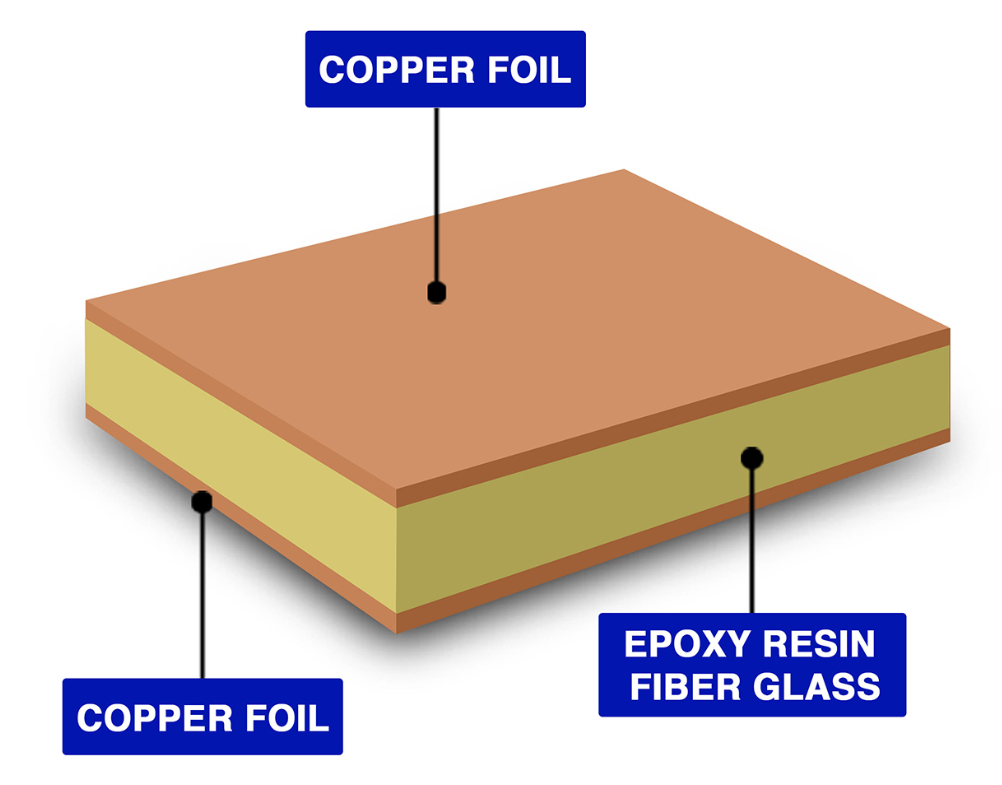
FR-4, a flame-retardant epoxy laminate, is the standard substrate for most PCBs due to its mechanical strength, electrical insulation, and thermal stability. It is widely favored in consumer electronics, automotive, and industrial applications. However, the cost of producing FR-4 PCBs can escalate quickly due to factors like material selection, complex layouts, and inefficient manufacturing processes. Cost optimization matters because it directly impacts project budgets and product competitiveness in the market. For electric engineers, reducing expenses without sacrificing quality ensures that designs remain viable for mass production. Addressing manufacturing costs and assembly costs through strategic planning also minimizes waste and enhances sustainability. Understanding these dynamics is the first step toward effective PCB cost reduction.
Technical Principles Behind FR-4 PCB Costs
Several factors contribute to the overall expense of FR-4 PCBs, spanning material choices to production techniques. Material selection plays a critical role, as FR-4 grades vary in resin content and glass weave, affecting both price and performance. Higher-quality laminates with better thermal properties often come at a premium, while standard grades suffice for less demanding applications. The PCB layout optimization process influences costs by determining the board's size, layer count, and trace complexity, all of which impact material usage and fabrication time.
Manufacturing costs rise with intricate designs requiring tight tolerances or additional processes like via drilling and plating. Assembly costs are affected by component density, soldering techniques, and the need for manual intervention. PCB panelization, the practice of arranging multiple boards on a single panel, also affects pricing by maximizing material utilization during production. Understanding these principles allows engineers to identify areas for cost savings while maintaining compliance with standards like IPC-6012E for rigid board performance.
Practical Solutions for PCB Cost Reduction
Achieving budget-conscious designs involves a combination of smart planning and technical adjustments. Below are proven strategies tailored for electric engineers focusing on FR-4 PCBs.
Optimize Material Selection for FR-4 BOM
Choosing the right FR-4 grade is essential for balancing cost and performance. Standard FR-4 materials meet the needs of most general-purpose applications, avoiding the expense of high-frequency or high-thermal grades unless necessary. Consult industry guidelines, such as IPC-4101E, to match material specifications with project requirements. Additionally, consider the thickness of the laminate. Thinner boards reduce material usage but must still meet mechanical stability standards. Collaborate with suppliers to source cost-effective options without compromising quality. A well-planned FR-4 BOM minimizes waste and ensures that only essential materials are procured.
Enhance PCB Layout Optimization
Efficient PCB layout optimization directly reduces manufacturing costs by minimizing board size and layer count. Place components strategically to shorten trace lengths, which lowers copper usage and simplifies routing. Avoid over-specifying tolerances unless critical to functionality, as tighter constraints increase production time and expense. Use design software to simulate and validate layouts before fabrication, ensuring errors are caught early. Reducing the number of vias and opting for simpler routing patterns also cuts costs. Adhering to design rules outlined in IPC-A-600K for acceptability of printed boards helps maintain manufacturability while keeping expenses in check.
Maximize PCB Panelization Efficiency
PCB panelization is a powerful technique for cost reduction during mass production. By arranging multiple identical boards on a single panel, material waste is minimized, and fabrication efficiency improves. Ensure that panel designs include proper spacing for cutting and depanelization processes to avoid damage. Use standard panel sizes compatible with manufacturing equipment to prevent additional setup fees. Incorporate fiducial marks and tooling holes as per IPC-6012E guidelines to aid in alignment during assembly. Effective panelization can significantly lower per-unit manufacturing costs, especially for high-volume runs.
Suggested Reading: Mastering Mouse Bites: A Comprehensive Guide to PCB Panelization
Minimize Layer Count Without Sacrificing Performance
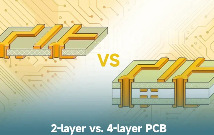
Reducing the number of layers in an FR-4 PCB is a direct way to cut expenses, as each additional layer increases material and processing costs. Evaluate whether a design can function with fewer layers by optimizing component placement and routing. For simpler circuits, a two-layer board may suffice instead of a four-layer configuration. Balance this approach with performance needs, ensuring signal integrity and thermal management are not compromised. Guidelines from IPC-2221B for generic PCB design standards can assist in making informed decisions about layer reduction.
Streamline Assembly Costs Through Design Choices
Assembly costs often account for a significant portion of PCB expenses, particularly with complex designs. Minimize these costs by designing for automated assembly wherever possible. Group similar components together to reduce pick-and-place machine setup time. Opt for surface-mount components over through-hole parts, as they are faster to assemble and require less manual labor. Ensure that component footprints comply with JEDEC J-STD-020E for moisture and reflow sensitivity to avoid assembly issues. Simplifying the design for assembly directly lowers labor and equipment costs.
Reduce Manufacturing Costs with Simplified Features
Complex features like blind vias, buried vias, or microvias drive up manufacturing costs due to additional processing steps. Stick to standard through-hole vias unless advanced features are critical to the design. Limit the use of fine-pitch components, as they require precise equipment and increase production time. Avoid unnecessary surface finishes if standard options like HASL (Hot Air Solder Leveling) meet the project needs. Following IPC-6012E standards ensures that designs remain within cost-effective manufacturing capabilities while meeting quality benchmarks.
Insight: Balancing Cost and Quality in FR-4 PCB Design
For electric engineers, the challenge lies in achieving PCB cost reduction without undermining reliability. A practical approach is to prioritize critical performance areas while applying cost-saving measures elsewhere. For instance, use premium PCB FR-4 material only in high-stress zones of the board, such as power supply sections, while opting for standard grades in less demanding areas. Simulate thermal and electrical performance during the design phase to identify potential failure points before production. Regularly review industry standards like IPC-A-600K to ensure that cost-driven decisions do not lead to defects or non-compliance. This balance allows for budget-conscious designs that still meet rigorous application demands.
Conclusion
Optimizing FR-4 PCB cost is a multifaceted process that demands attention to material selection, PCB layout optimization, and efficient manufacturing practices. By focusing on a streamlined FR-4 BOM, maximizing PCB panelization, and minimizing assembly costs, electric engineers can achieve significant savings. Practical strategies like reducing layer count and simplifying design features further contribute to lowering manufacturing costs. Balancing these cost-saving measures with adherence to industry standards ensures that quality remains uncompromised. Implementing these tips and tricks empowers designers to create budget-conscious designs while delivering reliable and high-performing FR-4 PCBs for diverse applications.
FAQs
Q1: How does material selection impact FR-4 PCB cost reduction?
A1: Material selection is crucial for FR-4 PCB cost reduction. Choosing standard FR-4 grades over specialized high-thermal or high-frequency options saves money for general applications. Thinner laminates reduce material usage but must meet mechanical needs. Following standards like IPC-4101E helps match materials to project requirements, ensuring cost efficiency without sacrificing reliability.
Q2: What role does PCB layout optimization play in lowering manufacturing costs?
A2: PCB layout optimization minimizes manufacturing costs by reducing board size, layer count, and routing complexity. Efficient component placement shortens traces, cutting copper usage. Avoiding tight tolerances unless necessary prevents added production time. Adhering to IPC-2221B design standards ensures layouts are cost-effective and manufacturable while maintaining performance.
Q3: How can PCB panelization help reduce assembly costs?
A3: PCB panelization lowers assembly costs by maximizing material use during production. Arranging multiple boards on a single panel reduces waste and speeds up fabrication. Proper spacing and alignment marks, as per IPC-6012E, streamline assembly processes. This approach is especially effective for high-volume runs, cutting per-unit expenses significantly.
Q4: Why is minimizing layer count important for budget-conscious PCB designs?
A4: Minimizing layer count directly reduces manufacturing costs since each layer adds material and processing expenses. Simplifying to a two-layer design from a four-layer one can save significant resources. Ensure signal integrity and thermal needs are met using IPC-2221B guidelines. This strategy supports budget-conscious designs without risking functionality.
References
IPC-6012E — Qualification and Performance Specification for Rigid Printed Boards. IPC, 2020.
IPC-A-600K — Acceptability of Printed Boards. IPC, 2020.
IPC-4101E — Specification for Base Materials for Rigid and Multilayer Printed Boards. IPC, 2017.
IPC-2221B — Generic Standard on Printed Board Design. IPC, 2012.
JEDEC J-STD-020E — Moisture/Reflow Sensitivity Classification for Nonhermetic Surface Mount Devices. JEDEC, 2014.


