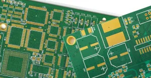
Why is Solder Mask Selection Crucial for High-Frequency PCBs?
A solder mask is a protective polymeric layer applied over the copper circuitry of a Printed Circuit Board (PCB). Its primary functions include preventing unintended solder bridging, shielding traces from oxidation, and ensuring solder adheres only to designated pads during assembly. While this protective coating is fundamental for all PCBs, its influence becomes significantly amplified in high-frequency applications, typically those operating above 1 GHz. At these elevated frequencies, even subtle material variations can introduce signal attenuation, distortion, or undesirable interference.
In environments demanding high-frequency operation—such as 5G telecommunications, advanced radar systems, and high-speed digital computing—maintaining signal integrity is paramount. The solder mask directly affects the electrical characteristics of the quick turn PCB, particularly through its dielectric constant (Dk) and dissipation factor (Df), also known as the loss tangent. An ill-chosen solder mask can introduce detrimental signal delays or energy losses, ultimately degrading the overall performance of the design. Therefore, prioritizing a high-frequency solder mask with minimal loss properties is a critical design consideration.
How Does Solder Mask Dielectric Constant (Dk) Influence Signal Integrity?
The dielectric constant (Dk) quantifies a material's capacity to store electrical energy within an electric field. For PCB materials, including the solder mask, a lower Dk value is generally more favorable for high-frequency applications. This preference stems from the fact that a higher Dk can impede signal propagation speed and elevate the risk of signal distortion.
Impact of Dk on High-Frequency Signals
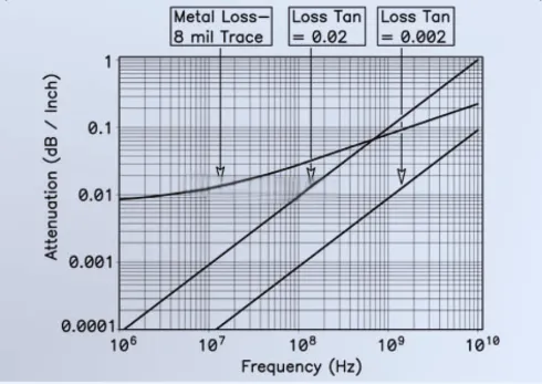
Standard solder masks typically exhibit a Dk ranging from 3.5 to 4.5. While adequate for lower-frequency designs, this range can cause considerable issues in circuits operating at 5 GHz or higher. At these frequencies, signals tend to propagate along the surface of the PCB, directly interacting with the solder mask layer. An elevated Dk can lead to impedance mismatches, which in turn cause signal reflections and energy loss. In contrast, specialized low-Dk solder masks can achieve values as low as 2.5 to 3.0, substantially mitigating these adverse effects.
Consider a design operating at 10 GHz: a solder mask with a Dk of 4.0 might introduce a noticeable delay in signal timing. Conversely, employing a low-Dk mask with a value of 2.8 could enhance timing accuracy by up to 10%. Such a difference can be decisive in precision-critical applications like advanced telecommunications infrastructure or automotive radar systems.
Why is a Low Loss Solder Mask Indispensable for High-Speed Designs?
Beyond the dielectric constant, the dissipation factor (Df), or loss tangent, of a solder mask plays a critical role in minimizing signal energy dissipation. The loss tangent quantifies the amount of electrical energy a material converts into heat when subjected to an alternating electric field. A higher Df indicates greater signal energy loss, directly compromising signal integrity in high-frequency circuits.
Minimizing Energy Loss
Conventional solder masks often have a Df between 0.02 and 0.03, which is generally considered too high for many modern high-frequency applications. Conversely, a low loss solder mask, characterized by a Df below 0.01, can dramatically reduce this energy dissipation. For instance, in a high-speed digital circuit transmitting data at 25 Gbps, the use of a low loss solder mask can decrease signal attenuation by up to 20%, thereby ensuring clearer and more dependable data transmission.
In essence, a low loss solder mask is a non-negotiable requirement for preserving signal integrity in high-frequency PCBs. It is crucial for maintaining strong signal strength and effectively reducing noise, which is vital for sophisticated applications such as advanced wireless communication systems or satellite technology.
What Types of Solder Mask Materials Are Optimal for High-Frequency PCBs?
Not all solder mask formulations offer comparable performance, especially when high-frequency designs are a consideration. The following discusses various types of solder mask materials and their suitability for minimizing signal loss and preserving signal integrity.
1. Epoxy-Based Solder Masks
Epoxy-based solder masks are the most widely utilized type in PCB manufacturing due to their cost-effectiveness and robust environmental protection. However, their typical dielectric constant of 3.8 to 4.5 and a loss tangent around 0.02 make them less suitable for demanding high-frequency applications. These materials are generally better reserved for low to mid-frequency designs where signal loss is not a primary concern.
2. Polyimide-Based Solder Masks
Polyimide solder masks offer a superior performance profile for the high-frequency PCB. They feature a lower dielectric constant, often in the range of 3.2 to 3.5, and a reduced loss tangent of approximately 0.01. This makes them a robust choice for applications extending up to 10 GHz. Additionally, polyimide masks exhibit excellent thermal stability, which is advantageous for designs exposed to elevated operating temperatures or thermal cycling.
3. Specialized Low-Dk/Low-Df Solder Masks
For the most stringent high-frequency requirements, particularly in cutting-edge technologies like 5G infrastructure and aerospace systems, specialized solder masks are available. These materials boast ultra-low dielectric constants (typically 2.5 to 3.0) and exceptionally low loss tangents (below 0.005). While they represent a higher investment, the significant enhancement in signal integrity often justifies the cost, especially for operations exceeding 20 GHz.
Practical Design Advice for Integrating High-Frequency Solder Masks
Selecting the appropriate solder mask material is only one part of the optimization process. The method of application and its integration into the overall PCB design are equally critical. Here are specific design recommendations to optimize your high-frequency solder mask for minimal signal loss and enhanced signal integrity.
Strategic Solder Mask Application
● Restrict Coverage on Critical Traces: In high-frequency designs, it is often beneficial to avoid applying solder mask directly over critical signal traces, particularly RF lines. Exposed traces exhibit reduced interaction with the mask's dielectric properties, thereby lowering the potential for signal distortion. If protection is absolutely necessary, consider an extremely thin layer of a low-Dk solder mask to strike a balance between protection and electrical performance.
● Achieve Impedance Matching: Precise impedance control is fundamental for high-frequency signals. An impedance mismatch between the PCB substrate and the solder mask can lead to signal reflections. For instance, if your substrate has a Dk of 3.0, pair it with a solder mask of similar or lower Dk to maintain a consistent characteristic impedance, typically targeting around 50 ohms for RF designs.
● Prototype Testing and Validation: Before committing to mass production, it is crucial to develop prototypes and rigorously test how your selected solder mask impacts signal integrity. Employ specialized instruments, such as a vector network analyzer, to accurately measure signal loss and reflection coefficients at your target operating frequencies. This proactive approach can save considerable time and expense by identifying and addressing potential issues at an early stage.
Addressing Challenges with High-Frequency Solder Masks
While low loss solder masks offer undeniable performance benefits, their implementation comes with specific challenges. Firstly, these specialized materials are generally more expensive than standard options, which can significantly impact project budgets. Secondly, some advanced low-Dk materials may exhibit suboptimal adhesion to certain substrate types, potentially leading to long-term reliability concerns.
Strategies for Overcoming Challenges
To mitigate cost implications, consider applying low loss solder masks selectively, only to the critical high-frequency sections of your PCB, while using more economical standard masks for less sensitive areas. Regarding adhesion issues, foster close collaboration with your PCB manufacturer to ensure optimal compatibility between the chosen solder mask and substrate materials. Furthermore, comprehensive testing under realistic operating conditions can help uncover and resolve any latent problems before final production.
Real-World Impact: How Solder Mask Affects Signal Integrity
Let's examine a practical scenario to underscore the importance of signal integrity solder mask. In the design of a 5G base station operating at 28 GHz, performance standards mandate that signal loss must not exceed 0.5 dB per inch. If a standard epoxy solder mask (Dk 4.0, Df 0.025) were used, the resulting loss could be as high as 0.8 dB per inch, failing to meet the specified requirement. However, by switching to a low loss solder mask (Dk 2.8, Df 0.005), the signal loss could be reduced to an acceptable 0.3 dB per inch, ensuring the design performs within specifications.
This example clearly illustrates how the careful selection of a high-frequency solder mask can be a decisive factor in the success or failure of a project. Whether you are designing for telecommunications, sophisticated medical imaging devices, or advanced automotive radar systems, meticulous attention to solder mask properties is an absolute necessity.
Future Outlook: Evolving Solder Mask Materials for High-Frequency Designs
As technological advancements continue apace, the demand for increasingly high-frequency PCBs is set to escalate. This trajectory necessitates a parallel evolution in solder mask materials. Researchers are actively developing new formulations aimed at achieving even lower dielectric constants and loss tangents, with aspirations of reaching Dk values below 2.0. Concurrently, the development of environmentally friendly solder masks that retain high-frequency performance is gaining momentum, aligning with global sustainability objectives.
Another emerging trend is the integration of solder mask application with advanced manufacturing techniques, such as additive processes. These innovative methods could enable more precise and localized application of solder masks, further minimizing their impact on critical high-frequency signal paths. Staying informed about these developments will undoubtedly provide designers with a competitive advantage in creating next-generation high-frequency PCBs.
Conclusion: Making Informed Choices for High-Frequency PCB Solder Masks
For high-frequency PCBs, the solder mask transcends its role as a mere protective layer; its dielectric constant, loss tangent, and overall material characteristics profoundly influence signal attenuation and integrity. By prioritizing a high-frequency solder mask with superior low-loss properties—such as those exhibiting a Dk below 3.0 and a Df below 0.01—you can achieve significant improvements in your design's electrical performance.
It is crucial to carefully consider the specific requirements of your application, conduct thorough testing with different materials, and meticulously optimize your design to strike an ideal balance between cost and performance. With the appropriate low loss solder mask and meticulous planning, you can effectively minimize signal loss and attain reliable, high-quality outcomes even in the most demanding high-frequency projects. AIVON is dedicated to supporting your endeavors with expert guidance and exceptional manufacturing solutions for all your PCB requirements.


