What Defines Dielectric Thickness in PCB Design?
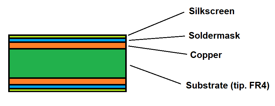
In the realm of Printed Circuit Board (PCB) design, dielectric thickness refers to the precise measurement of the insulating material situated between any two conductive layers, such as copper traces or extensive planes. This insulating layer, most commonly composed of materials like FR-4, plays a dual role: it physically prevents electrical short circuits between layers while profoundly influencing the manner in which electrical signals traverse the board. The intrinsic characteristics of this dielectric material, notably its thickness and dielectric constant (Dk), are pivotal in dictating the board's overall electrical performance.
Consider, for example, a typical 4 layer PCB stackup. Here, distinct dielectric layers meticulously separate the top signal layer from an internal ground plane, that ground plane from an underlying power plane, and so forth. The thickness of these intervening layers is not merely a matter of physical separation; it directly determines critical electrical parameters such as the characteristic impedance of transmission lines and the propagation delay of signals. A thinner dielectric can potentially reduce signal delays but may simultaneously amplify crosstalk between adjacent traces. Conversely, a thicker dielectric might lower capacitance but could also result in slower signal propagation speeds.
Why Dielectric Thickness is Crucial for Signal Integrity
Signal integrity fundamentally describes the quality and fidelity of an electrical signal as it travels across a PCB. If the dielectric thickness is not optimally designed, issues such as signal distortion, crosstalk, and timing discrepancies can readily emerge. This underscores why controlling PCB dielectric thickness is exceptionally critical for maintaining robust signal integrity.
● Impedance Control: Dielectric thickness directly dictates the characteristic impedance of transmission lines. For high-speed signals, achieving and maintaining a specific impedance (e.g., 50 ohms for many RF applications) is paramount to effectively prevent undesirable signal reflections that degrade performance.
● Signal Propagation Speed: Both the dielectric constant (Dk) and the thickness of the dielectric material significantly influence the velocity at which signals travel through the board. A thinner dielectric coupled with a lower Dk value facilitates faster signal propagation, a non-negotiable requirement for high-frequency designs.
● Crosstalk and Noise Mitigation: If the dielectric layers are insufficiently thick, signals on adjacent traces can detrimentally interfere with one another, leading to crosstalk. Appropriate dielectric thickness helps ensure adequate electrical isolation between distinct signal paths, minimizing unwanted noise.
Understanding and meticulously controlling dielectric thickness is therefore essential to guarantee the reliable performance of your PCB, especially within demanding applications such as advanced telecommunications or automotive electronics.
Dielectric Thickness and Impedance Control: An In-Depth Examination
One of the most profound impacts of dielectric thickness lies in its role in achieving precise dielectric thickness impedance control. This control is vital for ensuring that the electrical characteristics of a PCB trace perfectly align with the circuit's requirements, thereby minimizing deleterious signal reflections and power losses.
The characteristic impedance of any given trace is influenced by several interconnected factors, including:
● The dielectric thickness (the vertical distance separating the trace from its reference plane).
● The dielectric constant (Dk) of the chosen insulating material.
● The physical trace width and thickness.
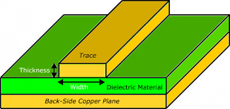
For example, consider a microstrip configuration, where a signal trace resides on the outermost surface of the PCB with a ground plane directly beneath it. In this setup, decreasing the dielectric thickness inherently increases the capacitance, which, in turn, reduces the characteristic impedance. A common target impedance for high-speed digital signals is 50 ohms. If, for instance, the dielectric thickness is 5 mils (0.005 inches) with a Dk of 4.2 (typical for standard FR-4), achieving a 50-ohm impedance might necessitate a trace width of approximately 9 mils, depending on other specific stack-up factors. However, if the dielectric thickness were to increase to 10 mils, the trace width would require adjustment to maintain the identical 50-ohm impedance target.
Designers routinely employ specialized impedance calculators or sophisticated simulation software to accurately determine the optimal dielectric thickness and corresponding trace dimensions. Without such precise control, any impedance mismatch can lead to severe signal reflections, ultimately causing data errors in sensitive high-speed circuits.
Standard FR-4 Dielectric Thickness Values in Industry
FR-4 remains the predominant dielectric material in PCB manufacturing, primarily due to its advantageous balance of cost-effectiveness and dependable performance. When discussing FR-4 dielectric thickness, it is important to differentiate between the overall board thickness and the thinner dielectric layers within a multilayer stack-up.
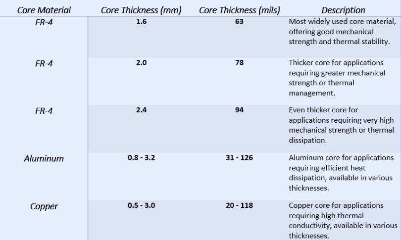
Standard overall FR-4 board thicknesses are commonly found at 0.062 inches (1.6 mm), 0.031 inches (0.8 mm), and 0.093 inches (2.4 mm). However, the dielectric thickness between individual layers in a multilayer PCB is considerably thinner. Typical dielectric thicknesses for FR-4 cores (pre-laminated panels) and prepregs (sheets of uncured epoxy resin and fiberglass used to bond layers) typically range from 3 mils (0.003 inches) to 20 mils (0.020 inches), chosen based on the total layer count and specific design imperatives.
For a common four-layer board, a representative stack-up might include:
● Top signal layer to first internal ground plane: 5 mils dielectric.
● Internal ground plane to internal power plane: 40 mils dielectric.
● Internal power plane to bottom signal layer: 5 mils dielectric.
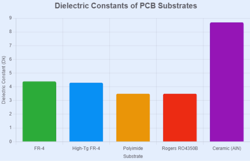
FR-4 possesses a dielectric constant (Dk) of approximately 4.2 to 4.5 at 1 MHz, though this value can fluctuate with frequency and variations among manufacturers. This Dk, in conjunction with the selected dielectric thickness, directly influences signal propagation speed and characteristic impedance. While FR-4 suffices for many standard designs, applications demanding very high frequencies (e.g., above 5 GHz) often necessitate specialized materials with lower Dk values.
Dielectric Considerations for High-Speed PCB Designs
In the realm of high-speed PCB dielectric designs, where signal frequencies frequently exceed 1 GHz or data transfer rates surpass 5 Gbps, the dielectric thickness assumes an even more paramount role. High-speed signals are inherently susceptible to increased losses, propagation delays, and unwanted interference; consequently, every aspect of the PCB stack-up requires meticulous planning.
Key considerations when designing for high-speed applications include:
● Thinner Dielectric Layers: Utilizing thinner dielectric layers can significantly reduce signal propagation delay and facilitate tighter impedance control. However, this approach often incurs higher manufacturing costs and may heighten the risk of crosstalk between adjacent layers.
● Materials with Low Dielectric Constant (Dk): While FR-4 is suitable for numerous applications, high-speed designs often mandate the use of advanced laminate materials boasting Dk values typically below 3.5. These specialized materials are chosen to minimize signal loss, which becomes increasingly critical at higher frequencies.
● Ensuring Uniform Thickness: Any minor variations in dielectric thickness across the board can lead to critical impedance mismatches, directly contributing to signal integrity issues. Therefore, demanding tight manufacturing tolerances for dielectric layers is essential.
For example, in a design operating at 10 Gbps, a mere 1 mil variation in dielectric thickness can induce a discernible shift in impedance, potentially resulting in bit errors. Designers must work in close collaboration with their PCB manufacturers to guarantee the consistent quality of dielectric layers, particularly within critical signal areas of the board.
Methods for Dielectric Thickness Calculation
Accurately calculating the appropriate dielectric thickness for your PCB is a pivotal step toward achieving optimal performance. While dielectric thickness calculation can be intricate, it generally involves determining the thickness required to meet specific impedance or signal speed objectives.
A simplified procedure for performing dielectric thickness calculation for a microstrip trace, aiming for a particular impedance, is as follows:
● Define Target Impedance: Clearly identify the characteristic impedance required (e.g., 50 ohms for many high-speed signals).
● Ascertain Dielectric Constant: Know the Dk value of your chosen material (e.g., 4.2 for standard FR-4).
● Estimate Trace Width: Begin with an approximate trace width, drawing from standard industry guidelines or insights from previous designs.
● Utilize an Impedance Formula or Software Tool: Employ a microstrip impedance formula or a dedicated calculator tool. A widely used approximation for microstrip impedance is based on the formula: Z = (87 / √(Dk + 1.41)) * ln(5.98 * H / (0.8 * W + T)), where H represents dielectric thickness, W is trace width, and T is trace thickness (all measurements typically in mils).
● Adjust Thickness Iteratively: Solve the formula for H (dielectric thickness) by inputting your desired Z and other known values. This process may require iteration to strike a balance with practical manufacturing constraints.
For illustrative purposes, to attain a 50-ohm impedance with a trace width of 10 mils and a trace thickness of 1.4 mils on an FR-4 material (Dk = 4.2), you might calculate a dielectric thickness of approximately 6 mils. However, in real-world engineering, sophisticated simulation tools are frequently necessary to achieve high accuracy, accounting for complex factors such as frequency-dependent Dk and inherent manufacturing tolerances.
Crucially, always engage in consultation with your online PCB manufacturer to confirm the actually achievable dielectric thicknesses, as the availability of standard prepreg and core materials may constrain your design choices. Furthermore, consider incorporating stack-up symmetry to mitigate the risk of board warping during the manufacturing process.
Practical Strategies for Optimizing Dielectric Thickness
Having covered the fundamental principles, here are actionable strategies to effectively optimize dielectric thickness within your PCB designs:
● Prioritize Standard Stack-Ups: Whenever feasible, begin with manufacturer-recommended stack-ups for common layer counts. This approach often simplifies the design process, reduces costs, and leverages established manufacturing capabilities. Only deviate from standard dielectric thicknesses if absolutely necessary to meet critical impedance or signal speed requirements.
● Simulate Before Physical Prototyping: Leverage advanced PCB design software to simulate signal behavior across various dielectric thickness configurations. This proactive step can reveal potential issues and validate design choices long before committing to expensive physical manufacturing.
● Account for Manufacturing Tolerances: Recognize that dielectric thickness can exhibit variations of ±10% or even more due to inherent manufacturing processes. Design your board with sufficient margin to accommodate these potential deviations, ensuring robust performance despite minor inconsistencies.
● Balance Cost with Performance Requirements: Understand that opting for thinner dielectrics and more advanced, specialized materials can indeed enhance performance but invariably leads to increased manufacturing costs. Carefully evaluate whether the performance benefits genuinely justify the additional expense for your specific application.
● Thorough Prototype Testing: For designs deemed critical or exceptionally sensitive, it is imperative to construct and rigorously test physical prototypes. This allows for direct measurement of actual impedance and signal integrity, providing empirical data to inform any necessary adjustments to dielectric thickness in subsequent design revisions.
Common Errors to Avoid Regarding Dielectric Thickness
Even highly experienced designers can inadvertently make mistakes when dealing with dielectric thickness. Being aware of these common pitfalls can prevent significant issues and costly rework.
One frequent error is ignoring frequency effects: the dielectric constant of materials like FR-4 is not static; it changes with frequency. Assuming a constant Dk value for high-speed designs can lead to inaccurate impedance calculations. Another critical mistake is overlooking stack-up symmetry: uneven dielectric thicknesses between layers can cause the board to warp during the high-temperature manufacturing process, leading to assembly problems. Neglecting crosstalk is also a significant concern; excessively thin dielectrics can lead to unacceptable signal interference between layers, compromising data integrity. Always ensure adequate spacing is maintained for your specific signal frequencies. Lastly, assuming uniform thickness across the entire board is a common misconception. Resin flow during the lamination process can introduce slight variations in dielectric thickness. Collaborating closely with your manufacturer is key to minimizing these inconsistencies and understanding their impact.
Conclusion: Mastering Dielectric Thickness for Superior PCB Performance
Dielectric thickness stands as a fundamental pillar of effective PCB design, directly influencing crucial aspects such as signal integrity, precise impedance control, and overall circuit performance. By thoroughly comprehending concepts like the critical role of PCB dielectric thickness for signal integrity, becoming proficient in dielectric thickness impedance control, and adeptly applying appropriate FR-4 dielectric thickness standards or advanced high-speed PCB dielectric strategies, designers can consistently create highly reliable and efficient circuit layouts. Furthermore, acquiring proficiency in dielectric thickness calculation methods empowers you to meticulously fine-tune your PCB stack-ups to meet even the most stringent performance requirements.
Whether your project involves designing a straightforward two-layer board or engineering a complex, high-speed multi-layer system, paying meticulous attention to dielectric thickness is paramount. It ensures that your electrical signals propagate cleanly and without undesirable interference, maintaining their fidelity from source to destination. Leverage the practical tips and profound insights presented in this guide to significantly elevate the quality of your PCB designs, and always foster a collaborative relationship with your manufacturing partner to achieve the absolute best possible outcomes.
With a well-informed and strategic approach, you can confidently master the intricacies of dielectric thickness, thereby enabling you to construct PCBs that not only meet but exceed the rigorous demands of contemporary electronics. Continue to experiment, rigorously test, and continually refine your designs to remain at the forefront of this ever-evolving technological field.


