Introduction
In the realm of high-speed electronic design, achieving precise signal integrity is a critical challenge for electrical engineers. One key aspect is optimizing the PCB stackup for differential impedance control, which ensures reliable data transmission in modern circuits. Differential impedance stackup design directly impacts the performance of high-speed signals, minimizing noise and crosstalk in differential pair routing. A well-planned controlled impedance PCB stackup design addresses these issues by aligning layer arrangements with impedance requirements. This guide provides a structured approach to impedance calculation for differential pairs, focusing on practical strategies for PCB layer arrangements. By understanding and applying these principles, engineers can enhance circuit performance and meet stringent industry standards. The following sections break down the essentials of stackup design and offer actionable insights for optimal results.
What Is Differential Impedance and Why It Matters
Differential impedance refers to the impedance between two traces in a differential pair, which carry signals of equal magnitude but opposite polarity. This parameter is vital in high-speed designs, as it influences signal integrity and reduces electromagnetic interference. Unlike single-ended impedance, differential impedance stackup accounts for the coupling between traces, making PCB layer arrangements a critical factor. Properly controlled impedance PCB stackup design ensures that signals maintain their integrity over long distances, especially in applications like USB, HDMI, and Ethernet.
The importance of differential impedance lies in its ability to minimize noise. When impedance mismatches occur, reflections can degrade signal quality, leading to data errors. For electrical engineers, mastering impedance calculation for differential pairs is essential to meet performance specifications. A poorly designed stackup can introduce crosstalk or signal loss, impacting overall system reliability. Thus, a strategic approach to stackup design is non-negotiable in modern electronics.
Technical Principles of Differential Impedance Control
Differential impedance control hinges on the interaction between trace geometry, dielectric materials, and PCB layer arrangements. The impedance of a differential pair is determined by the trace width, spacing, and the dielectric constant of the material between layers. Additionally, the proximity to reference planes, typically ground or power layers, plays a significant role in maintaining consistent impedance.
The fundamental principle involves maintaining a specific differential impedance value, often 90 or 100 ohms, depending on the protocol. This requires precise impedance calculation for differential pairs, factoring in the stackup configuration. For instance, placing differential pairs closer to a reference plane reduces loop inductance, stabilizing impedance. Engineers must also consider the dielectric thickness between layers, as it affects the electric field distribution around traces.
Crosstalk is another concern in differential pair routing. Tight coupling between traces in a pair helps reject common-mode noise, but excessive spacing from reference planes can weaken this effect. Industry standards, such as IPC-2141A, provide guidelines for designing controlled impedance PCB stackup structures. Adhering to these ensures that signal paths are optimized for minimal interference.
Key Factors in PCB Stackup Design for Impedance Control
Layer Arrangements and Symmetry
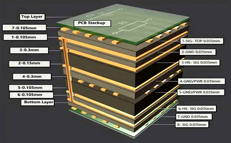
PCB layer arrangements are the backbone of controlled impedance design. A symmetrical stackup, where dielectric layers are evenly distributed, helps maintain consistent impedance across the board. For differential pairs, placing signal layers adjacent to continuous reference planes is a common practice. This configuration provides a stable return path for high-speed signals, reducing impedance variations.
A typical four-layer stackup might include a top signal layer, a ground plane, a power plane, and a bottom signal layer. In such designs, differential pairs on the top or bottom layer benefit from proximity to the ground plane. For multilayer boards, alternating signal and plane layers further enhances control over differential impedance stackup. Engineers must avoid routing differential pairs across split planes, as this disrupts the return path and alters impedance.
Dielectric Material Selection
The choice of dielectric material impacts impedance due to its dielectric constant and loss tangent. Materials with a lower dielectric constant allow for wider traces or thinner dielectrics to achieve the same impedance, which can simplify manufacturing. Consistency in material properties across layers is crucial for accurate impedance calculation for differential pairs. Variations in dielectric thickness or composition can lead to mismatches, affecting signal integrity.
Trace Geometry and Spacing
Trace width and spacing are pivotal in differential pair routing. Narrower traces increase impedance, while closer spacing between pairs reduces it due to stronger coupling. Engineers often use field solvers or simulation tools to determine optimal dimensions based on the target differential impedance. Maintaining uniform spacing and avoiding sharp bends in traces preserves signal quality during routing.
Related Reading: Designing for Signal Integrity: Mastering 50 Ohm PCB Impedance Control
Practical Steps for Optimizing PCB Stackup Design
Step 1: Define Impedance Requirements
Begin by identifying the required differential impedance for your design, based on the communication protocol or application. Common values range from 85 to 120 ohms, depending on standards like USB or PCIe. Document these requirements clearly to guide the stackup design process. This step ensures that all subsequent decisions align with the target impedance.
Step 2: Select an Appropriate Layer Count
Choose a layer count that supports controlled impedance PCB stackup design. For simpler designs, a four-layer board may suffice, with signal layers adjacent to ground planes. Complex high-speed designs often require six or more layers to accommodate multiple differential pairs and dedicated reference planes. Ensure that the layer count balances cost and performance needs.
Step 3: Plan Layer Arrangements
Arrange layers to prioritize signal integrity. Place differential pairs on outer layers or internal signal layers close to continuous reference planes. Avoid stacking multiple signal layers without intervening planes, as this increases crosstalk risks. Symmetry in layer arrangements also aids in minimizing board warpage during fabrication, maintaining consistent impedance.
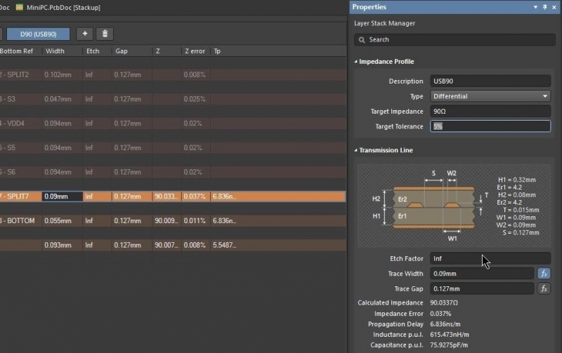
Step 4: Perform Impedance Calculations
Conduct impedance calculation for differential pairs using established formulas or simulation tools. Account for trace width, spacing, dielectric thickness, and material properties. Standards like IPC-2141A offer guidance on these calculations, ensuring accuracy. Verify the results against the target impedance to confirm the stackup meets design goals.
Step 5: Validate with Fabrication Constraints
Collaborate with the fabrication team to ensure the stackup design is manufacturable. Confirm dielectric thicknesses and material availability, as deviations can alter impedance. Specify tolerances for trace dimensions and layer spacing to maintain controlled impedance during production. This step prevents costly redesigns due to manufacturing limitations.
Best Practices for Differential Pair Routing
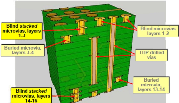
Effective differential pair routing complements a well-designed stackup. Keep traces of a pair closely coupled with consistent spacing to maintain impedance. Route pairs away from high-noise areas, such as switching power supplies, to avoid interference. Use vias sparingly, as they introduce discontinuities that can disrupt impedance.
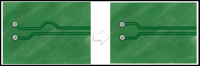
Matching the length of traces in a differential pair is critical for timing accuracy. Length mismatches can cause skew, degrading signal quality. When routing across layers, ensure vias are placed symmetrically for both traces to preserve coupling. Following guidelines from standards like IPC-2221B helps achieve reliable routing outcomes.
Additionally, maintain a clear return path by avoiding cuts or splits in reference planes beneath differential pairs. A solid ground plane adjacent to the signal layer ensures minimal loop area, stabilizing impedance. These practices, combined with a robust stackup, enhance overall design performance.
Related Reading: Mastering Differential Pair Routing for High-Speed PCB Design
Common Challenges and Troubleshooting Tips
Designing for differential impedance stackup often presents challenges like impedance mismatches or crosstalk. One frequent issue is variation in dielectric thickness during fabrication, which alters impedance. To address this, specify tight tolerances for layer spacing and verify material consistency before production.
Crosstalk between adjacent differential pairs can degrade performance. Increasing spacing between pairs or adding ground traces as shields mitigates this problem. If simulation shows impedance deviations, revisit trace geometry or adjust layer arrangements to correct the issue. Regularly consult standards like IPC-A-600K for acceptability criteria during troubleshooting.
Another concern is signal reflection due to improper termination. Ensure termination resistors match the differential impedance to minimize reflections. By anticipating these challenges and applying systematic solutions, engineers can maintain controlled impedance across the design lifecycle.
Conclusion
Optimizing PCB stackup for differential impedance control is a cornerstone of high-speed design. By focusing on controlled impedance PCB stackup design, engineers can ensure signal integrity and reduce noise in differential pair routing. This guide has outlined the technical principles, practical steps, and best practices for achieving precise impedance calculation for differential pairs. Proper PCB layer arrangements, material selection, and routing techniques are essential to meeting performance goals. Adhering to industry standards and validating designs against fabrication constraints further enhances reliability. With a structured approach, electrical engineers can tackle the complexities of differential impedance stackup and deliver robust, high-performance circuits for demanding applications.
FAQs
QX: What is differential impedance stackup, and why is it important for high-speed designs?
AX: Differential impedance stackup refers to the configuration of PCB layers to maintain specific impedance between differential pairs. It is crucial for high-speed designs because it ensures signal integrity by minimizing noise and crosstalk. A well-designed stackup prevents reflections and data errors, supporting reliable communication in protocols like USB or Ethernet. Following industry standards helps achieve consistent performance.
QX: How does controlled impedance PCB stackup design impact signal integrity?
AX: Controlled impedance PCB stackup design directly affects signal integrity by maintaining uniform impedance across differential pairs. Proper layer arrangements and dielectric materials reduce signal loss and interference. This design approach prevents mismatches that cause reflections, ensuring clean signal transmission. It is a fundamental aspect of high-speed circuit reliability, guided by recognized standards.
QX: What are the key factors in differential pair routing for impedance control?
AX: Differential pair routing for impedance control requires close trace coupling and consistent spacing to maintain impedance. Traces should avoid noisy areas and use minimal vias to prevent discontinuities. Length matching is vital to avoid skew, and solid reference planes ensure stable return paths. These practices enhance signal quality in high-speed applications.
QX: How is impedance calculation for differential pairs performed in PCB design?
AX: Impedance calculation for differential pairs involves analyzing trace width, spacing, dielectric thickness, and material properties. Engineers use formulas or simulation tools to determine the values, aligning them with target impedance. Standards like IPC-2141A provide guidelines for accuracy. This process ensures the stackup supports the required differential impedance for optimal performance.
IPC-2141A - Design Guide for High-Speed Controlled Impedance Circuit Boards. IPC, 2004.
IPC-2221B - Generic Standard on Printed Board Design. IPC, 2012.
IPC-A-600K - Acceptability of Printed Boards. IPC, 2020.