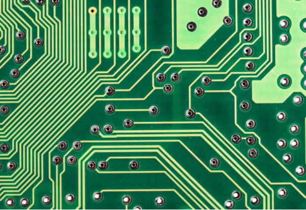
What is PCB Trace Clearance and Why is it Essential?
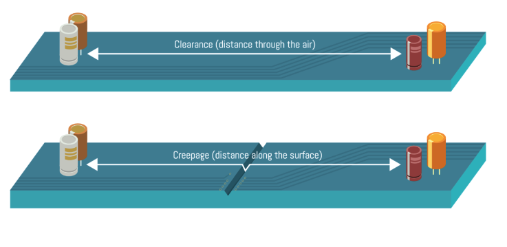
PCB trace clearance refers to the physical separation distance between any two conductive elements on a circuit board, such as traces, pads, or vias. This spacing is a critical design parameter because it directly impacts the board's operational safety, electrical performance, and ease of manufacturing. Insufficient spacing can lead to detrimental issues like electrical arcing, short circuits, or unwanted interference between signals, all of which can result in system failures. Conversely, excessively wide spacing, while safe, can squander valuable board real estate, diminishing the design's overall efficiency.
For engineers and designers, establishing and maintaining the correct minimum trace spacing is a delicate balance. It's about ensuring the PCB functions reliably across a range of conditions, whether for a simple low-power circuit or a sophisticated high-speed system. Factors such as voltage potentials, signal speeds, and ambient environmental conditions all play a significant role in determining the appropriate clearance. By adhering to established PCB design rules, designers can proactively prevent problems like crosstalk and uphold signal integrity, topics we will explore in detail.
Minimum Trace Spacing Guidelines in PCB Design
Minimum trace spacing specifies the smallest permissible distance between any two conductive elements, as dictated by stringent PCB design rules. This critical dimension varies widely, depending on the specific application and its operational requirements. For example, a low-voltage consumer electronic device might only demand a few mils (thousandths of an inch) of clearance, while a high-voltage industrial application could necessitate several millimeters to prevent dangerous electrical arcing.
Primary Reasons for Proper Trace Spacing
● Safety Assurance: Adequate spacing is fundamental in preventing electrical shorts or hazardous arcing, particularly in high-voltage designs where greater clearances (a rough guideline is often 0.1mm per 100V) are indispensable.
● Signal Integrity Maintenance: Correct spacing minimizes interference between adjacent traces, ensuring that electrical signals remain clean, clear, and undistorted. This is especially vital in high-speed circuits operating at frequencies exceeding 100 MHz.
● Manufacturability: Proper spacing guarantees that the PCB can be fabricated without defects. Overly tight spacing can introduce significant production errors during critical stages such as etching or soldering, leading to costly reworks or scrap.
Design rules governing trace spacing are frequently guided by robust industry standards, such as those published by the Institute of Printed Circuits (IPC). For instance, IPC-2221, a widely recognized standard, offers comprehensive guidelines for clearances based on specific voltage levels. For a circuit operating at 50V, an external layer might require a minimum clearance of 0.6mm (approximately 24 mils), with even greater spacing mandated for higher voltage applications.
Key Factors Affecting PCB Trace Clearance
Several critical factors dictate the minimum clearance needed between traces. A thorough understanding of these influences empowers designers to make informed decisions, ensuring optimal PCB performance throughout the design phase.
Key Influencing Factors
● Voltage Potentials: The voltage difference between neighboring traces is a primary determinant. Higher voltages substantially increase the risk of electrical breakdown or arcing through the air or across the board’s insulating surface. As a general principle, clearance must proportionally increase with voltage. For example, a 100V design might require a minimum of 1mm of spacing, whereas a 500V application could demand 2.5mm or more, depending on the specific board material and environmental context.
● Signal Speed and Frequency: In high-speed designs, preserving signal integrity becomes paramount. High-frequency signals, particularly those exceeding 1 GHz, can readily couple with adjacent traces if spacing is insufficient, resulting in disruptive crosstalk. To counteract this, designers often implement wider spacing or strategically interpose ground planes between high-speed signal traces. A commonly cited rule-of-thumb is to maintain a spacing of at least three times the trace width for high-speed signals to minimize unwanted interference.
● Environmental Conditions: Ambient factors such as humidity, temperature, and altitude can significantly impact the required clearance. In environments with high humidity, moisture can degrade the insulating properties of both air and the board material, thereby heightening the risk of arcing. In such conditions, designers might increase standard clearance recommendations by 20-30% to ensure sustained reliability.
● Board Material and Layer Configuration: The specific type of substrate material used (e.g., FR-4) and the PCB's overall layer stackup also influence clearance requirements. Internal layers typically permit tighter spacing due to the consistent insulating material surrounding them, while external layers demand greater clearance due to their exposure to air and potential contaminants. For example, an internal layer clearance for a 50V circuit might be as low as 0.1mm, in contrast to the 0.6mm required for external layers.
Essential PCB Design Rules for Minimum Trace Spacing
To achieve optimal PCB performance and ensure reliability, it is absolutely crucial to adhere to established design rules for trace spacing. These guidelines serve as a fundamental blueprint for creating robust and efficient circuit board designs.
Critical Design Guidelines
● Comply with Industry Standards: Always consult and apply industry standards such as IPC-2221 for general clearance guidelines. For instance, for a 150V design, this standard typically suggests a minimum clearance of 0.7mm on external layers under standard operating conditions.
● Acknowledge Manufacturing Limitations: Crucially, verify the minimum spacing capabilities of your chosen PCB fabrication house. While many standard manufacturing processes can reliably handle 6-mil (0.15mm) spacing, designs requiring tighter clearances may necessitate more advanced and potentially costlier fabrication techniques.
● Differentiate by Net Class: Implement distinct clearance rules for different categories of signals. For example, power traces might require a minimum of 0.5mm spacing, whereas high-speed data lines could demand 1mm or more to effectively prevent crosstalk.
● Utilize Design Software Tools: Leverage the capabilities of modern PCB design software, which often include integrated Design Rule Checks (DRC). These tools can automatically flag any clearance violations. Configure these rules precisely based on your project's specific voltage, frequency, and environmental requirements.
By diligently following these PCB design rules, you can effectively circumvent common design pitfalls and ensure that your circuit board design meets both its functional and safety requirements.
Suggested Reading: How to Calculate Optimal Trace Spacing in PCB Design
How Proper Spacing Prevents Crosstalk and Ensures Signal Integrity
Signal integrity refers to the overall quality and reliability of electrical signals as they propagate through a fast turn PCB. Poor signal integrity can manifest as data errors, critical timing inaccuracies, or even complete system failure, particularly in high-speed applications. A leading cause of signal degradation is crosstalk, a phenomenon where signals from one trace undesirably interfere with another due to insufficient physical separation.
Strategies for Signal Integrity and Crosstalk Prevention
● Increased Spacing for High-Speed Signals: For critical high-speed signals, such as those found in USB 3.0 or DDR memory circuits, maintaining a minimum spacing of at least three times the trace width (often referred to as the "3W rule") is highly effective. For example, a 5-mil wide trace would ideally require a minimum spacing of 15 mils. This increased separation effectively minimizes the electromagnetic coupling—both electric and magnetic fields—that causes crosstalk.
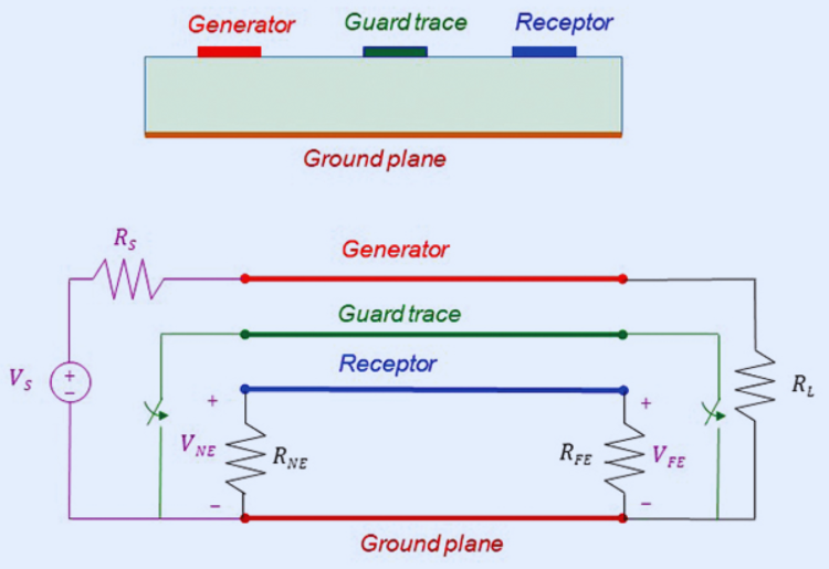
● Strategic Use of Ground Planes or Guard Traces: Interposing a continuous ground plane or a grounded guard trace between high-speed signal traces can further significantly reduce interference. A guard trace, typically positioned at least 5 mils from the signal traces, acts as an effective electromagnetic shield, absorbing unwanted energy. This technique is particularly beneficial in designs where frequencies exceed 500 MHz.
● Routing Critical Signals on Separate Layers: When board space is severely limited, consider routing high-speed or highly sensitive signals on different layers, with a dedicated ground plane situated between them. This approach effectively increases the perceived clearance and physically isolates the signals, thereby preserving their integrity. For instance, separating a 2.4 GHz RF signal from a digital control line on different layers can prevent interference that would otherwise occur with only 0.2mm of spacing on the same layer.
Common Mistakes in PCB Trace Clearance and How to Avoid Them
Even seasoned designers can inadvertently make errors when setting trace clearances. Being aware of these common pitfalls and understanding how to prevent them can save considerable time and resources.
Preventing Design Errors
● Ignoring Voltage Ratings: Failing to adequately account for peak voltages can lead to critically insufficient clearance, increasing the risk of arcing. Always design for the absolute maximum expected voltage, and, as a safety measure, incorporate an additional safety margin of 10-20% beyond recommended spacing guidelines.
● Overlooking High-Speed Requirements: Not increasing trace spacing for high-frequency signals is a frequent cause of crosstalk. Utilize advanced simulation tools to accurately predict potential interference and adjust spacing parameters accordingly before fabrication.
● Neglecting Fabrication Limits: Designing with clearances that fall below your chosen manufacturer's capabilities will inevitably lead to production failures. For standard circuit boards, it is generally advisable to avoid spacing below 6 mils (0.15mm) unless you have explicit confirmation of your manufacturer's advanced process capabilities.
Practical Strategies for Optimizing PCB Trace Clearance
Designing with optimal trace clearance doesn't have to be an overwhelming task. Implementing these actionable tips can significantly streamline the process and lead to more robust designs.
Actionable Optimization Tips
● Develop a Clearance Matrix: Create a structured table detailing all clearance requirements, categorized by voltage levels, signal types, and specific layers. For example, define 0.3mm for low-voltage signals on internal layers and 1mm for high-voltage traces on external layers.
● Leverage Simulation Tools: Actively use specialized software to simulate electric fields and predict signal behavior across your board. This proactive approach can help identify and mitigate potential crosstalk issues long before physical fabrication begins.
● Iterate and Rigorously Test: Always build the quick PCB prototype to test your design under real-world operating conditions. Employ an oscilloscope to accurately measure signal integrity and confirm that your chosen clearance values are effective and meet performance expectations.
Conclusion: Mastering PCB Trace Clearance for Superior Designs
A profound understanding and precise implementation of minimum trace clearance stand as a cornerstone of effective PCB design. By prioritizing appropriate trace spacing, you can significantly enhance signal integrity, prevent detrimental crosstalk, and ultimately ensure the inherent safety and long-term reliability of your electronic circuits. Whether your project involves a low-power gadget or a complex high-speed communication device, adhering to established PCB design rules and meticulously considering factors such as voltage, signal frequency, and environmental conditions will invariably lead to optimal performance.
With a well-informed approach to PCB trace clearance, you can proactively circumvent common design pitfalls and craft circuit boards that impeccably meet both their intended functional requirements and critical manufacturing specifications. Keep these comprehensive guidelines at the forefront of your mind during your next project to achieve an ideal balance between design efficiency and unwavering reliability, thereby ensuring your innovations endure the test of time.