What Are Plated Through-Holes (PTH) and Their Importance in High-Speed PCBs?
For engineers engaged in designing high-speed printed circuit boards (PCBs), a thorough command of plated through-hole (PTH) design is absolutely critical for maintaining signal integrity and optimizing overall performance. PTH vias serve as essential conductive pathways connecting different layers within a PCB. However, in high-speed applications, if not meticulously designed, they can introduce significant challenges such as impedance mismatches and detrimental signal delays. This comprehensive guide will delve into advanced PTH design rules, strategies for managing high-speed PCB vias, techniques for impedance control in PTH, methods for ensuring signal integrity with plated through-holes, and best practices for differential pair routing utilizing PTH. Whether you are an experienced engineer or new to the field of PCB design, this resource offers practical advice and detailed insights to help you perfect your high-speed PCB layouts.
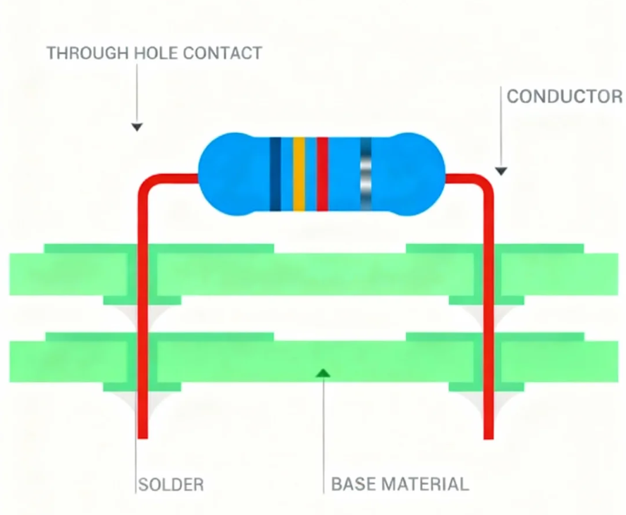
Plated through-holes are precisely drilled, conductive holes extending through a PCB, engineered to establish electrical connections between various layers. Unlike non-plated holes, PTHs are characterized by a thin layer of copper plated on their interior walls, ensuring robust and reliable conductivity. In high-speed PCBs, where signals often operate at frequencies exceeding 1 GHz, PTH vias play a pivotal role in preserving signal quality. Poorly designed PTHs can regrettably lead to signal reflections, increased crosstalk, and significant signal loss, all of which can ultimately result in system failures. In high-speed design, every element, including vias, exerts an influence on performance. Consequently, PTH vias must be planned with extreme care to minimize any disruptions to the signal paths. We will now explore how to design them effectively, emphasizing key aspects such as impedance control, signal integrity, and optimized routing strategies.
Essential PTH Design Rules for High-Speed PCBs
Designing PTH vias for high-speed PCBs demands strict adherence to specific rules to prevent performance degradation. The following guidelines represent the most crucial principles to integrate into your design process.
Minimizing Via Stub Lengths
In high-speed designs, via stubs—which are the unused segments of a via that extend beyond the layer where the signal transitions—act as parasitic antennas, generating unwanted signal reflections. For signals operating at frequencies such as 5 GHz, a stub exceeding just 0.5 mm in length can introduce substantial noise and signal degradation. To mitigate this, consider employing back-drilling techniques to physically remove these unused stub sections. Alternatively, if your PCB stack-up and design constraints allow, opt for blind or buried vias, which inherently eliminate stubs.
Optimizing Via Diameter and Pad Size
The physical dimensions of vias directly impact their electrical characteristics. Smaller via diameters generally lead to reduced parasitic capacitance and inductance, both of which are critical for maintaining signal integrity at elevated frequencies. A typical via diameter for high-speed designs ranges from 0.2 mm to 0.3 mm, often accompanied by pad sizes of approximately 0.5 mm to 0.6 mm. It is crucial to ensure that the chosen via size can adequately support the required current-carrying capacity while simultaneously minimizing signal distortion.
Strategic Placement of Vias
It is best practice to avoid placing PTH vias directly within the path of high-speed signals unless absolutely necessary. When a via is unavoidable, position it strategically to minimize any disruption to the trace length. For instance, placing vias at the termination point of a trace, rather than in its mid-section, can significantly reduce signal path interruptions and reflections.
Achieving Impedance Control with PTH in High-Speed Designs
Impedance control forms a cornerstone of high-speed PCB design. PTH vias, if not managed correctly, can unfortunately disrupt the characteristic impedance of a signal path. Here’s how to ensure effective impedance control when utilizing PTH.
Matching Via Impedance to Trace Impedance
High-speed signals frequently necessitate a carefully controlled impedance, typically 50 ohms for single-ended traces and 100 ohms for differential pairs. A PTH via inherently introduces parasitic inductance and capacitance, which can alter this impedance. To counteract this effect, it's essential to meticulously adjust the via pad size and the anti-pad (the clearance area in the ground plane surrounding the via). For a 50-ohm trace, an anti-pad diameter typically ranging from 0.8 mm to 1.0 mm often yields good results, although precise values should always be derived through simulation tools tailored to your specific PCB stack-up.
Incorporating Ground Vias for Return Paths
Strategically placing ground vias in close proximity to high-speed signal vias is crucial for establishing a low-impedance return path. This practice effectively reduces loop inductance and minimizes electromagnetic interference (EMI). A common guideline is to place at least one ground via for every signal via, ideally within a 1 mm radius, to ensure a robust return current path.
Simulating Via Effects for Precision
Utilizing electromagnetic simulation software is highly recommended to accurately model the impedance characteristics of PTH vias within your design. These advanced tools can predict how vias will affect signal behavior at frequencies exceeding 1 GHz, enabling you to fine-tune critical parameters such as via spacing and pad size before committing to physical fabrication, thereby preventing costly revisions.
Ensuring Signal Integrity with Plated Through-Holes
Signal integrity pertains to the maintenance of a signal's quality as it propagates through a quick turn PCB. PTH vias, if not meticulously designed, can significantly degrade signal integrity. The following strategies are vital for preserving signal integrity in high-speed designs.
Mitigating Crosstalk Through Proper Spacing
Crosstalk, an undesirable phenomenon where signals in adjacent vias interfere with one another, must be minimized. To prevent this, maintain a minimum spacing of at least three times the via diameter between high-speed signal vias. For example, if using a 0.3 mm via diameter, ensure a spacing of 0.9 mm or greater. This separation helps to isolate electromagnetic fields and reduce coupling.
Limiting Via Transitions in Critical Nets
Each instance a signal transitions through a via to a different layer, it encounters impedance discontinuities. For critical high-speed nets, it is imperative to limit the number of such via transitions. If transitions are unavoidable, ensure that the via is adequately surrounded by a solid ground plane; this provides a stable reference and minimizes the introduction of noise and reflections.
Utilizing High-Quality Dielectric Materials
The dielectric material of your PCB significantly influences how signals behave, particularly around PTH vias. For designs operating at frequencies above 10 GHz, employing low-loss materials with a low dielectric constant (Dk) (typically 3.0 to 3.5) is highly recommended, as these materials effectively reduce signal attenuation and dispersion, particularly in the vicinity of vias.
Differential Pair Routing with PTH in High-Speed PCBs
Differential pairs are a common feature in high-speed designs for various protocols like USB, PCIe, and Ethernet. They utilize two complementary signals to effectively reduce noise. Routing these pairs through PTH vias demands exceptional precision to maintain signal balance and accurate timing. Here’s how to execute it correctly.
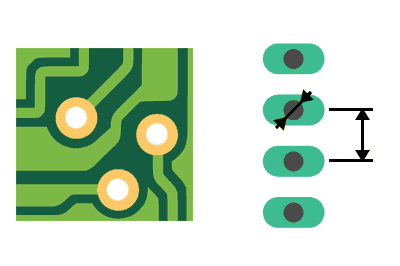
Maintaining Differential Via Symmetry
When routing differential pairs, it is crucial to place the vias for each pair as close together as possible while strictly maintaining symmetry. Asymmetrical spacing can lead to signal skew, where one signal arrives before the other, thereby disrupting critical timing. For signals operating up to 5 GHz, a spacing of 0.5 mm to 0.8 mm between differential vias often yields optimal results.
Matching Trace Lengths Across Via Transitions
Length mismatches within differential pairs introduce phase differences, which can significantly degrade signal integrity and overall performance. Therefore, it is essential to ensure that the trace lengths on both sides of the vias are precisely equal. If a length discrepancy is unavoidable due to via placement, employ serpentine routing techniques to meticulously match the lengths, ideally to within 0.1 mm.
Encircling Differential Vias with Ground Planes
To effectively shield differential pairs from external noise and interference, it is recommended to place ground vias strategically around the pair. This creates a localized, controlled electromagnetic environment, substantially reducing both EMI and crosstalk. A common and effective practice for signals exceeding 3 GHz is to form a ring of four to six ground vias surrounding the differential pair vias.
Advanced Strategies for High-Speed PCB Vias and PTH Design
Beyond the fundamental principles, several advanced strategies can further refine PTH design in the high-speed and high frequency PCB, pushing performance boundaries.
Advanced Via Techniques
● Blind and Buried Vias: Employing blind vias (connecting an outer layer to an inner layer) and buried vias (connecting only inner layers) fundamentally eliminates stubs, which dramatically improves signal integrity. While these specialized vias typically increase fabrication costs, their performance benefits often justify the investment for designs operating above 10 GHz.
● Via Stitching for Ground Planes: Via stitching involves strategically placing multiple ground vias around high-speed signal paths to establish a robust and low-inductance return path. This technique is particularly effective in multilayer boards where signals may traverse multiple layers via PTH vias. To suppress unwanted resonances, space stitching vias at intervals approximately equal to λ/10, where λ represents the wavelength of the highest signal frequency.
● Rigorous Testing and Validation: Following the PCB design phase, utilize time-domain reflectometry (TDR) to accurately measure impedance discontinuities introduced by PTH vias. This proactive testing helps identify and rectify issues such as reflections or mismatches before full-scale production, thereby saving both time and cost.
Common Pitfalls to Avoid in PTH Design for High-Speed PCBs
Even seasoned designers can inadvertently make errors when working with PTH vias in high-speed applications. Being aware of these common pitfalls can help prevent costly mistakes.
Design Mistakes
● Ignoring Via Stubs: Failing to address and manage via stubs can lead to severe signal reflections, a particularly detrimental issue at frequencies exceeding 1 GHz.
● Overcrowding Vias: Placing an excessive number of vias too close together significantly increases the risk of crosstalk and complicates subsequent routing efforts.
● Neglecting Robust Ground Planes: Without a solid and continuous ground plane in close proximity to vias, return paths become elongated, leading to increased inductance and heightened electromagnetic interference (EMI).
● Bypassing Simulations: Omitting electromagnetic simulations for via effects can result in unforeseen performance issues that prove expensive and time-consuming to correct after physical fabrication.
Conclusion: Achieving High-Speed PCB Success Through Mastered PTH Design
Mastering plated through-hole (PTH) design is an absolutely critical aspect of developing high-speed PCBs. By diligently adhering to established PTH design rules, maintaining stringent impedance control, ensuring robust signal integrity, and optimizing differential pair routing, you can engineer circuit boards that deliver reliable and high-performance operation even at the most demanding frequencies. Always prioritize minimizing via stubs, strategically utilizing ground vias to establish effective return paths, and rigorously simulating your designs to identify and resolve potential issues in the early stages. Equipped with these comprehensive strategies, you will be exceptionally well-prepared to tackle the complexities of high-speed PCB design and consistently deliver superior results.


