Introduction
In the world of printed circuit board design, achieving optimal circuit performance is a priority for electronic hobbyists and professionals alike. A key factor in this pursuit is the proper configuration of power and ground planes within the PCB stackup. These planes play a critical role in maintaining signal integrity, reducing noise, and improving stability in electronic circuits. For DIY electronics enthusiasts, understanding how to structure power ground planes in a PCB can transform a noisy, unstable design into a reliable one. This article explores the importance of power and ground planes, their impact on circuit performance stackup, and practical strategies for reducing noise and enhancing stability. Whether you are working on a simple project or a complex multilayer board, these insights will help elevate your designs.
What Are Power and Ground Planes and Why Do They Matter
Power and ground planes are dedicated layers in a PCB stackup that distribute electrical power and provide a reference for signals. Unlike traces that carry specific signals, these planes cover large areas of the board to ensure uniform voltage distribution and a stable return path for currents. In any PCB, the power plane supplies voltage to components, while the ground plane acts as a common return path, minimizing interference.
Their importance cannot be overstated. Properly designed power ground planes in a PCB reduce electromagnetic interference, prevent voltage drops, and enhance overall circuit performance stackup. For hobbyists working on DIY electronics performance, poor plane design can lead to issues like signal crosstalk or unstable operation. By prioritizing these layers, you create a foundation for reducing noise in power planes and improving stability with ground planes, ensuring your circuits function as intended.
Related Reading: PCB Grounding Techniques: A Guide to Minimizing Noise and Ensuring Reliable Connections
Technical Principles of Power and Ground Planes in PCB Stackup
Understanding the role of power and ground planes requires a grasp of basic electrical principles. These layers form a low impedance path for current, which is essential for maintaining consistent voltage levels across the board. When a component draws current, the power plane supplies it with minimal resistance, while the ground plane offers a direct return path, avoiding loops that could induce noise.
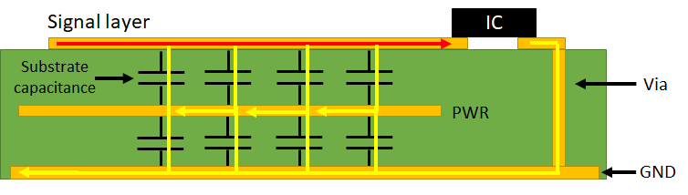
One critical aspect is capacitance between adjacent power and ground planes. When placed close together in the stackup, these layers act as a natural capacitor, helping to filter high frequency noise. This inherent decoupling effect is vital for reducing noise in power planes, especially in high speed digital circuits common in DIY electronics performance projects. Additionally, a well designed ground plane minimizes ground bounce, a phenomenon where voltage fluctuations occur due to rapid switching of digital signals.
Another principle is the management of electromagnetic interference. Ground planes act as shields, absorbing stray electromagnetic fields that could interfere with sensitive signals. Positioning them strategically in the stackup enhances their ability to improve stability with ground planes, protecting your circuit from external or internal noise sources.
Impact of Stackup Configuration on Circuit Performance
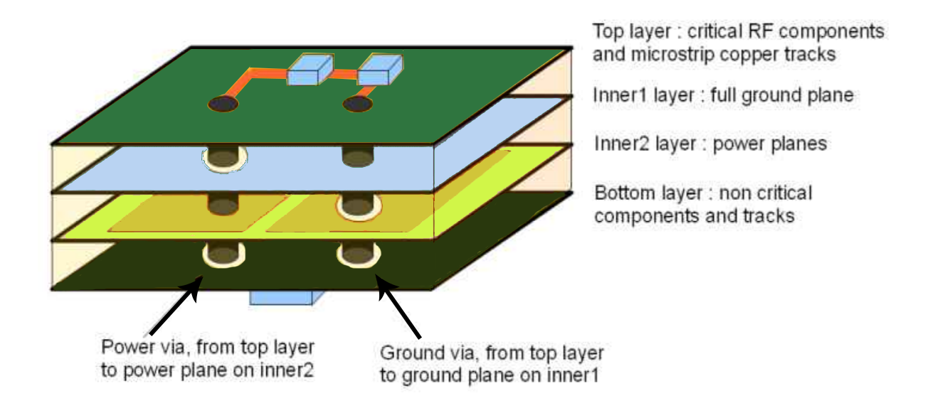
The arrangement of layers in a PCB stackup directly influences circuit performance stackup. For hobbyists, even a simple four layer board can benefit from thoughtful design. A common approach is to dedicate inner layers to power and ground planes, sandwiching them between signal layers on the outer surfaces. This configuration reduces noise by keeping high speed signals close to a reference plane, minimizing loop areas where interference can develop.
In multilayer designs, placing power and ground planes adjacent to each other enhances the capacitive coupling mentioned earlier. This setup is particularly effective for reducing noise in power planes, as it helps stabilize voltage during sudden current demands. However, incorrect stackup can lead to issues. For instance, if a ground plane is too far from a signal layer, return currents may take longer paths, increasing noise and degrading performance.
Hobbyists should also consider layer thickness and dielectric materials between planes. Thinner dielectrics increase capacitance, aiding noise suppression, but they must comply with manufacturing capabilities. Following industry guidelines, such as those outlined in IPC-6012E, ensures that stackup designs meet performance and reliability standards.
Related Reading: Power and Ground Plane Design in 4 Layer PCBs
Practical Solutions for Optimizing Power and Ground Planes
Optimizing power ground planes in a PCB is achievable with practical steps tailored for electronic hobbyists. Below are actionable strategies to enhance circuit performance stackup and address common challenges like noise and stability.
Prioritize Ground Plane Continuity
A continuous ground plane is essential for providing a low impedance return path. Avoid splitting the ground plane unless absolutely necessary for isolating analog and digital sections. Breaks in the plane can force return currents to detour, increasing noise and reducing stability. If splits are needed, use stitching capacitors to bridge the sections, maintaining a consistent reference.
Place Power and Ground Planes Close Together
In multilayer stackups, position power and ground planes on adjacent layers to maximize capacitance. This setup acts as a built in decoupling mechanism, crucial for reducing noise in power planes. For hobbyists using four layer boards, a common stackup is signal, ground, power, and signal. This arrangement ensures signals have a nearby reference while benefiting from plane capacitance.
Use Decoupling Capacitors Effectively
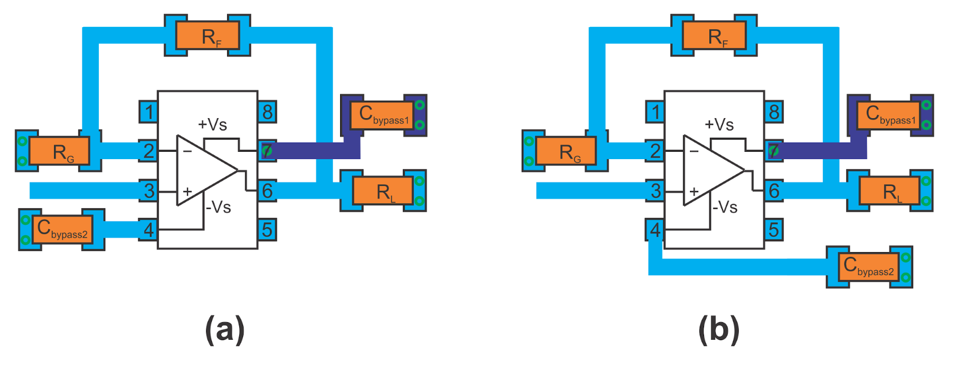
Decoupling capacitors are vital for stabilizing voltage near components. Place them as close as possible to power pins of integrated circuits to filter transient noise. Select capacitor values based on the frequency range of your circuit, ensuring they address both low and high frequency noise. This practice directly supports improving stability with ground planes by minimizing voltage fluctuations.
Minimize Loop Areas in Signal Routing
When routing signals, keep traces short and direct, especially for high speed lines. Large loop areas between signal traces and their return path on the ground plane can induce noise. Route critical signals over a solid ground plane to ensure the shortest return path, enhancing DIY electronics performance.
Follow Industry Standards for Design
Adhering to established guidelines ensures reliability. The IPC-2221B standard provides recommendations for layer spacing and plane design in PCBs. For hobbyists, consulting such standards helps avoid common pitfalls in stackup design, ensuring that power ground planes in a PCB are optimized for performance.
Troubleshooting Common Issues with Power and Ground Planes
Even with careful planning, issues can arise in power and ground plane design. Hobbyists often encounter noise or instability, which can disrupt circuit performance stackup. Here are common problems and solutions.
One frequent issue is excessive noise due to inadequate decoupling. If your circuit exhibits erratic behavior, check the placement and value of decoupling capacitors. Ensure they are near component pins and cover the necessary frequency spectrum. Adding more capacitors in parallel can address a broader range of noise frequencies.
Another problem is ground bounce in high speed designs. This occurs when multiple components switch simultaneously, causing voltage spikes on the ground plane. To mitigate this, use a solid ground plane and minimize via transitions for critical signals. Stitching vias around the board perimeter can also reinforce ground continuity, aiding in reducing noise in power planes.
Finally, improper stackup can lead to signal integrity issues. If signals cross multiple layers without a nearby reference plane, crosstalk can occur. Review your stackup to ensure each signal layer is adjacent to a ground or power plane. Adjusting the layer order may resolve such problems, improving stability with ground planes.
Conclusion
Optimizing power and ground planes in a PCB stackup is a fundamental step for electronic hobbyists aiming to achieve superior circuit performance. These layers are not just passive components but active contributors to reducing noise, enhancing stability, and ensuring reliable operation. By understanding the principles behind power ground planes in a PCB, prioritizing thoughtful stackup design, and applying practical solutions like decoupling and plane continuity, you can significantly improve DIY electronics performance. Following industry standards such as IPC-2221B and IPC-6012E further ensures that your designs meet professional benchmarks. With these strategies, your circuits will operate more efficiently, paving the way for successful projects.
FAQs
Q1: How do power ground planes in a PCB improve circuit performance stackup?
A1: Power and ground planes provide stable voltage distribution and a low impedance return path for currents. This setup minimizes voltage drops and noise, directly enhancing circuit performance stackup. For hobbyists, a well designed plane configuration ensures signals remain clean, reducing errors in digital or analog circuits. Following proper layout practices is key to achieving these benefits.
Q2: What are effective ways for reducing noise in power planes during DIY projects?
A2: Reducing noise in power planes involves placing decoupling capacitors near component pins and ensuring power and ground planes are adjacent in the stackup. Use continuous ground planes to avoid return path disruptions. For DIY electronics, keeping signal traces short and over reference planes also helps minimize interference and maintain signal integrity.
Q3: How does improving stability with ground planes impact overall circuit reliability?
A3: Improving stability with ground planes creates a consistent reference for signals, preventing ground bounce and voltage fluctuations. This reduces the risk of erratic behavior in components, boosting circuit reliability. For hobbyists, a solid ground plane design means fewer unexpected failures, ensuring your DIY electronics performance remains predictable even under varying conditions.
Q4: Why is stackup design critical for DIY electronics performance?
A4: Stackup design determines how layers interact, affecting noise and signal integrity in your PCB. A balanced arrangement with power and ground planes near signal layers minimizes interference and supports stable operation. For DIY electronics performance, proper stackup ensures your circuits handle high speeds or sensitive signals without issues, leading to successful builds.
References
IPC-2221B — Generic Standard on Printed Board Design. IPC, 2012.
IPC-6012E — Qualification and Performance Specification for Rigid Printed Boards. IPC, 2020.


