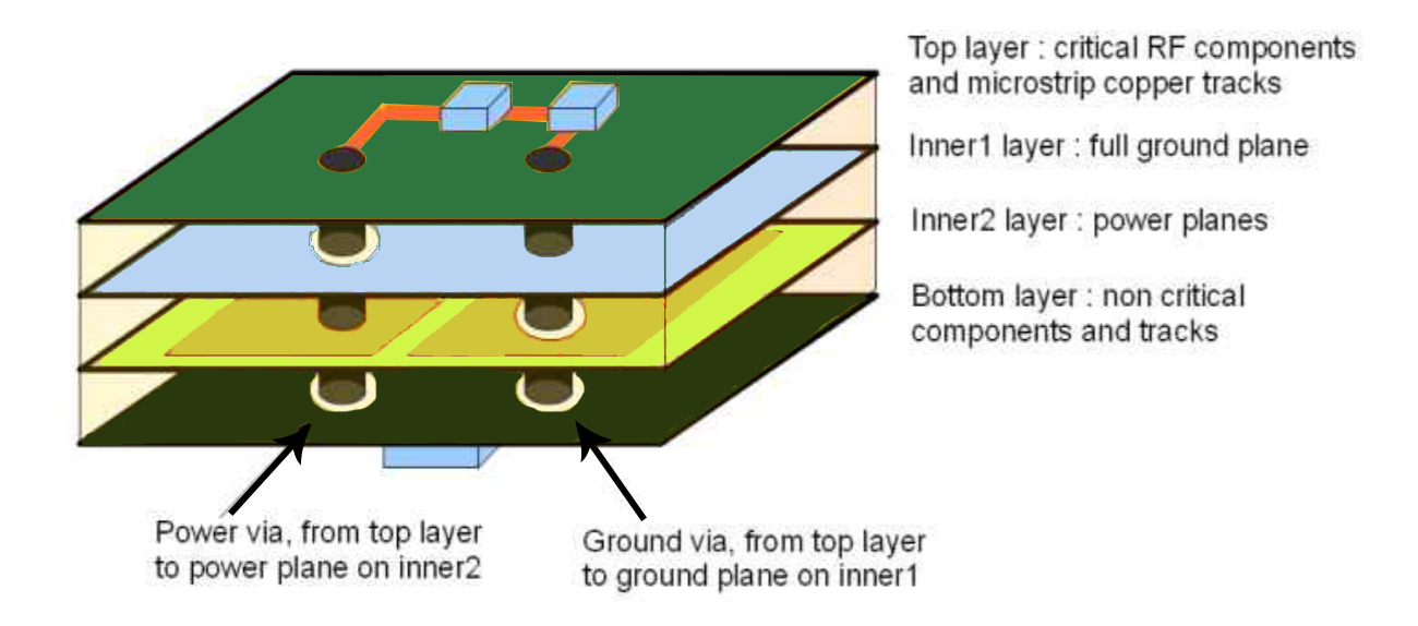
Why Are Power Plane Vias Essential in PCB Design?
Power plane vias are small, conductive pathways linking power and ground planes across different layers within a Printed Circuit Board (PCB). They serve a critical function by ensuring stable power delivery to components and establishing a consistent reference for electrical signals. Without their careful implementation, these vias can inadvertently introduce electrical noise, increase inductance, and degrade the overall signal integrity, particularly in circuits operating at high speeds or handling significant currents.
Signal integrity fundamentally describes the quality of an electrical signal as it propagates through a circuit. Issues like data corruption, timing inaccuracies, and electromagnetic interference (EMI) can arise from poor signal integrity. By strategically optimizing the placement of power plane vias, designers can establish a low-impedance path for power, effectively minimizing unwanted noise and ensuring that signals remain clear and dependable throughout the circuit.
How Does Power Plane Via Stitching Improve Performance?
Power plane via stitching is a technique that involves precisely placing multiple vias across a quick turn PCB to interconnect power or ground planes between various layers. This method is fundamental for establishing a resilient power distribution network (PDN) and effectively reducing impedance. Via stitching helps to mitigate voltage drops, ensures a more uniform current distribution, and lowers EMI by providing numerous low-resistance pathways for current flow.
Strategic Stitching in High-Speed Designs
In designs that operate at high frequencies, via stitching becomes particularly crucial, especially around components that draw high current, such as microprocessors or FPGAs. For instance, arranging vias at consistent intervals (e.g., every 0.5 inches) around a power plane can significantly decrease loop inductance and guarantee a stable voltage supply. Without adequate stitching, there's a risk of creating "hot spots" where current density becomes excessively high, potentially leading to overheating or degradation of signal quality. AIVON engineers emphasize uniform grid patterns for balanced current distribution and recommend placing vias as close as possible to component power pins to shorten current travel distances.
What is the Current Capacity of Power Plane Vias?
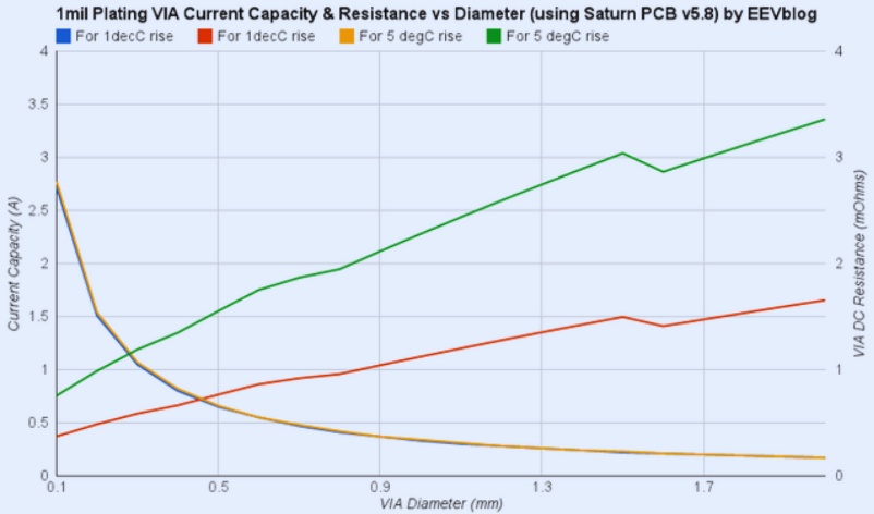
The current-carrying capacity of a power plane via is a critical design consideration, influenced by its diameter, the thickness of its copper plating, and the materials used in its construction. A typical via, approximately 10 mils (0.010 inches) in diameter with standard copper plating, can generally support about 1-2 amperes of current safely. However, for applications demanding higher currents, designers might need to opt for larger vias or incorporate multiple vias in parallel to effectively distribute the electrical load.
Calculating and Managing Current Flow
To accurately determine a via's current capacity, designers often rely on established industry formulas or specific PCB design guidelines. The current capacity scales with the via's cross-sectional area; for example, doubling a via's diameter can increase its current handling capability fourfold. However, thermal considerations are equally vital. Excessive current flowing through a via can cause significant overheating, which compromises reliability. A good practice is to maintain current density below 500 A/in² to prevent thermal stress and ensure long-term stability.
How Does Via Inductance Impact Signal Integrity?
Inductance within power plane vias is a major concern for maintaining signal integrity, especially in high-speed circuit designs. This inductance can cause unwanted voltage fluctuations and delay the delivery of power to components, ultimately leading to signal distortion. A via's inductance is determined by its length, diameter, and its proximity to other conductive elements. Generally, a shorter and wider via will exhibit lower inductance.
For example, a typical via measuring 50 mils in length and 10 mils in diameter might have an inductance of approximately 1-2 nH (nanohenries). While this value may seem minimal, in high-frequency circuits operating at 1 GHz or higher, even a small amount of inductance can create substantial impedance, thereby disrupting consistent power delivery. To mitigate this, best practices involve using the shortest possible via lengths by connecting power planes on adjacent layers and employing multiple vias in parallel to reduce the overall effective inductance. For signals critical to high-speed performance, the goal is to achieve via inductance below 0.5 nH through optimized via sizing and careful layer stackup design.
What Are the Key Guidelines for Power Plane Via Placement?
Strategic via placement is foundational for preserving signal integrity in PCB designs. Incorrectly positioned vias can introduce noise, increase impedance, and contribute to ground bounce. Adhering to specific guidelines for power plane vias is crucial for optimal performance:
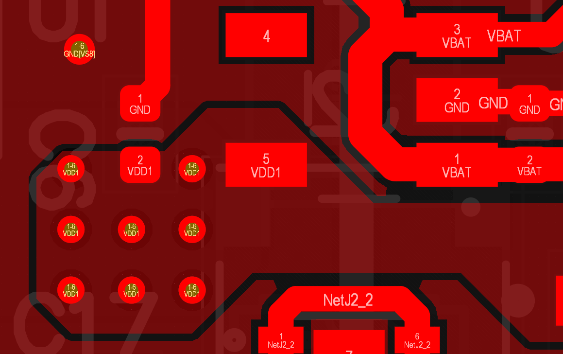
● Proximity to Power Pins: Place power plane vias as close as possible to the power pins of integrated circuits (ICs) and other components drawing high current. This minimizes the loop area, effectively reducing inductance and improving power delivery.
● Multiple Vias for High Current: For components that require more than 1 ampere, utilize multiple vias in parallel. This approach ensures even current distribution and mitigates thermal stress on individual vias.
● Avoid Signal Paths: Keep power plane vias separate from high-speed signal traces to prevent interference. If unavoidable, ensure a robust ground plane is nearby to provide shielding.
● Regular Ground Plane Stitching: In the multilayer circuit board, stitch ground planes with vias at consistent intervals (e.g., every 0.2-0.5 inches). This maintains a low-impedance return path for signals.
● Consider Via Aspect Ratio: Ensure that the ratio of a via’s height to its diameter (aspect ratio) remains below 10:1. This helps maintain manufacturability and reliability, as high aspect ratios can lead to plating defects.
What About Signal Integrity Vias and Common Mistakes?
Special Considerations for Signal Integrity Vias
Signal integrity vias are specifically designed to preserve the quality of high-speed signals by providing a clear return path and reducing crosstalk. Unlike power plane vias, which primarily focus on current delivery, signal integrity vias are often positioned near differential pairs or high-speed traces to precisely control impedance and minimize reflections. For example, in a design with a 10 Gbps signal, placing ground vias adjacent to signal vias can help maintain a controlled impedance of 50 ohms, thereby reducing signal distortion. Furthermore, signal integrity vias should be symmetrically placed around differential pairs to ensure balanced return paths and prevent signal skew.
Common Pitfalls in Power Plane Via Design
Even experienced designers can encounter challenges with power plane via placement. A common mistake is insufficient via stitching, where not enough vias are used for power or ground planes, leading to high impedance and significant voltage drops. Another pitfall is overloading a single via with high current, which can cause overheating and premature failure; distributing the load across multiple vias is key. Ignoring layer transitions also proves problematic, as poorly planned via transitions between layers can introduce unwanted inductance and disrupt signal integrity. Finally, neglecting thermal management for high-current vias, which generate substantial heat, can lead to reliability issues if proper spacing or thermal vias aren't considered.
Tools and Techniques for Optimizing Via Placement
Modern PCB design software provides powerful functionalities to refine the placement of power plane vias. Features such as auto-placement algorithms, integrated impedance calculators, and thermal analysis tools can significantly streamline the design process. Furthermore, conducting simulations for both signal integrity and power distribution is crucial for identifying and resolving potential issues well before the manufacturing phase.
For instance, simulating a power plane with vias spaced at varying intervals can reveal the optimal configuration to minimize voltage drops. A common objective is to limit voltage ripple to less than 1% of the supply voltage (e.g., 50 mV for a 5V rail) by adjusting the number and position of vias. A practical tip is to always utilize design rule checks (DRC) to confirm that all vias adhere to manufacturing constraints, such as minimum spacing and aspect ratio, to prevent any fabrication complications.
Conclusion: Mastering Power Plane Vias for Robust PCB Performance
Optimizing the placement of power plane vias is a foundational aspect of achieving superior signal integrity in PCB designs. By carefully considering power plane via stitching, understanding the current capacity of vias, minimizing via inductance, and adhering to established placement guidelines, designers can construct a resilient power distribution network that supports clean signals and ensures reliable circuit performance. Whether the application involves high-speed digital circuits or high-current power supplies, the core principles of signal integrity vias remain constant: meticulous planning, strategic placement, and an unwavering attention to detail.
Embracing the actionable advice and best practices outlined in this guide will equip you to confidently address the complexities of power plane via design. Implementing these strategies will not only elevate the performance and stability of your PCBs but also significantly reduce the likelihood and cost of needing expensive redesigns. Continued experimentation with various layouts and simulations is encouraged to strike the perfect balance for your specific application.


