Why Is Careful Via Spacing Essential in High-Speed PCB Design?
In the intricate world of printed circuit board (PCB) design, vias serve as vital conduits, enabling signals to transition between different layers. However, in the realm of high-speed electronics, where signals pulse at gigahertz frequencies, the arrangement of these vias becomes a critical factor for maintaining signal integrity. Inadequately spaced vias can introduce a host of problems, including electromagnetic interference and signal degradation.
Signal integrity fundamentally refers to the fidelity of an electrical signal as it traverses the PCB. Challenges such as crosstalk, where signals inadvertently interfere with one another, or return loss, which occurs when impedance mismatches cause signal reflections, can severely impair performance. Thoughtfully optimizing via-to-via spacing is key to mitigating these issues, ensuring that signals remain clear and robust, even when operating at very high speeds.
What Signal Integrity Challenges Do Vias Introduce in High-Speed PCBs?
High-speed PCBs, ubiquitous in modern technology from telecommunications to consumer gadgets, operate at frequencies where minor design flaws can lead to significant operational issues. Understanding the specific challenges related to via placement and signal integrity is crucial.
Crosstalk and Electromagnetic Interference Concerns
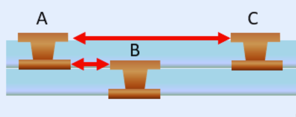
Crosstalk manifests as interference between signals due to electromagnetic coupling, leading to distorted data and potential errors in high-speed systems. Vias positioned too close together can inadvertently function as miniature antennas, picking up unwanted signals from adjacent vias or traces. Research indicates that crosstalk can escalate significantly—by over 20%—if via spacing falls below a specific critical distance. This threshold is typically around 3 to 5 times the via's diameter, influenced by factors such as the dielectric material and the signal's operating frequency.
Impedance Discrepancies and Return Loss
Effective impedance control is vital for preventing signal reflections. Vias inherently introduce discontinuities in the signal path, which can alter impedance. When vias are not spaced optimally, these discontinuities become more pronounced, resulting in increased return loss. For example, at frequencies around 5 GHz, a via spacing below 0.5 mm on a standard FR-4 board can elevate return loss by up to 10 dB, severely compromising signal quality.
Signal Propagation Delay and Timing Precision
In high-speed designs, precise timing is non-negotiable. Closely packed vias can contribute to parasitic capacitance and inductance, which collectively slow down signal propagation. This added delay can desynchronize data streams, posing particular challenges for applications like DDR memory or high-speed serial links operating at 10 Gbps or higher.
What Are the Best Practices for Optimizing Via Spacing in High-Speed Designs?
To overcome the inherent challenges, adopting specific strategies for via spacing can significantly enhance signal integrity. These practices are geared towards meticulous via impedance control, effective return loss minimization, and robust crosstalk reduction.
Tailoring Via Spacing to Signal Frequency
The optimal separation between vias is highly dependent on the signal's operating frequency. A general guideline is that higher frequencies necessitate greater spacing to lessen coupling effects. For signals exceeding 1 GHz, maintaining a separation of at least 3 to 5 times the via's diameter is recommended. For instance, if a via has a diameter of 0.2 mm, aim for a spacing between 0.6 mm and 1.0 mm. For designs operating at 10 GHz, this might need to increase to 1.2 mm or more to keep crosstalk below acceptable levels, typically around -30 dB.
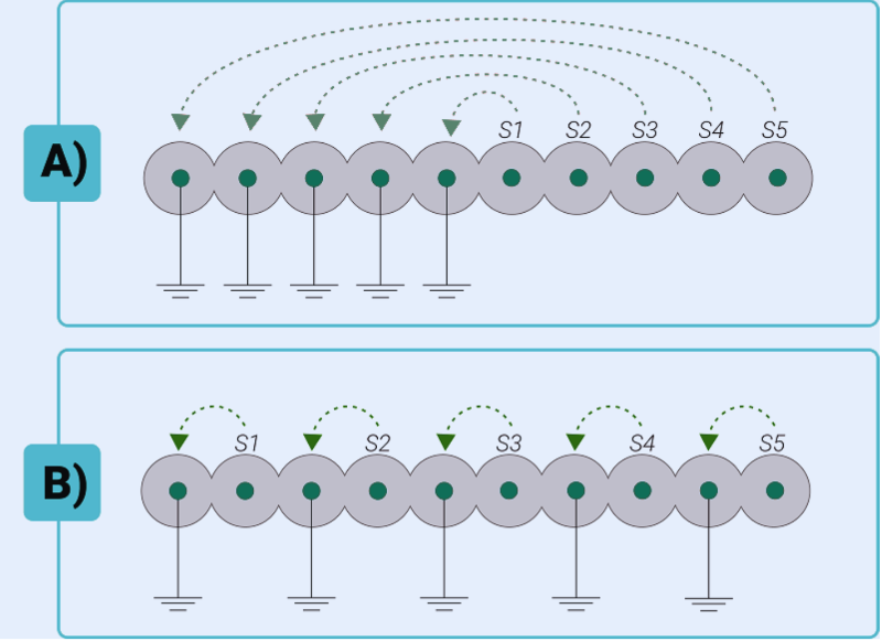
Employing Ground Vias for Enhanced Shielding
Strategically placing ground vias near signal vias can act as an electromagnetic shield, effectively reducing crosstalk. These ground vias establish a robust return path for high-speed signals, thereby minimizing unwanted electromagnetic interference. A common technique involves surrounding critical signal vias with ground vias, typically at a distance of about 1.5 to 2 times the signal via diameter. This approach can reduce crosstalk by 15-20% in designs running at 5 GHz or higher.
Achieving Via Impedance Control Through Meticulous Design
Controlling via impedance is crucial for mitigating return loss. Design engineers should utilize simulation tools to accurately model the impedance of vias, considering their diameter, length, and relative spacing. For example, a via with a 0.3 mm diameter and 1.6 mm length in a four-layer PCB might achieve an impedance close to 50 ohms if designed correctly. Adjusting the spacing to prevent clustering helps maintain this desired impedance, thereby preventing signal reflections. Keeping return loss below -10 dB often necessitates precise adjustments to via placement during the layout phase.
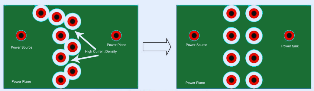
Strategic Trace Routing Away from Via Clusters
It is advisable to avoid routing high-speed traces in close proximity to densely packed via clusters. The electromagnetic fields radiating from vias can couple with nearby traces, leading to signal distortion. If routing near vias is unavoidable, ensure a minimum separation of at least three trace widths. Additionally, consider using differential pairs, which can inherently cancel out common-mode interference. This practice is particularly vital for signals operating at speeds above 2.5 Gbps.
Minimizing Via Stub Lengths
Via stubs, which are unused segments of a via extending beyond the active signal path, can function as resonant structures. These stubs can amplify noise and increase return loss at specific frequencies. Techniques like back-drilling or the use of blind and buried vias are critical for eliminating stubs in paths carrying high-speed signals. For a 10 GHz signal, a stub as short as 0.5 mm can noticeably increase return loss, potentially exceeding -5 dB.
Advanced Strategies for Reducing Crosstalk and Optimizing Return Loss
Beyond fundamental spacing rules, advanced design techniques, often requiring sophisticated simulation software and careful planning, can significantly boost performance in high-speed PCB designs.
Designing Vias for Differential Pairs
Differential pairs are frequently employed in high-speed serial links for data transmission. When incorporating vias into differential pair designs, maintaining perfect symmetry in their spacing and placement is essential to ensure balanced impedance. Even a minor spacing mismatch of 0.1 mm between differential vias can introduce skew, degrading signal integrity at speeds above 5 Gbps. It is crucial to keep the via-to-via spacing within the differential pair tight—approximately 1.5 times the via diameter—while ensuring the entire pair is sufficiently separated from other signals, typically by at least three times that distance.
Leveraging Simulation and Modeling for Via Spacing Optimization
Simulation tools are indispensable for fine-tuning via spacing. Specialized software can model electromagnetic fields, accurately predict crosstalk levels, and calculate return loss for various via configurations. For instance, at 8 GHz, simulations might reveal that a via spacing of 0.8 mm results in crosstalk of -35 dB, whereas reducing it to 0.4 mm could dramatically increase crosstalk to -20 dB. These insights are vital for refining the design prior to manufacturing.
Optimizing the PCB Layer Stackup
The PCB layer stackup significantly influences how vias interact with signal paths. High-speed signals should ideally be routed on layers that have continuous ground planes, which provide a stable return current path. It is important to avoid placing vias too close to the edges of ground planes, as this can disrupt the return current flow and increase return loss. A meticulously designed six-layer stackup with dedicated ground and power planes, for example, can reduce crosstalk by up to 10% compared to a less optimally planned layout.
How Does Material Selection Impact High-Speed PCB Performance?
The choice of PCB substrate material also plays a critical role in determining optimal via spacing and overall signal integrity. Standard PCB FR-4 material, with a typical dielectric constant (Dk) of around 4.2, is generally suitable for frequencies up to about 1 GHz. For applications involving higher frequencies, however, considering low-loss materials with a Dk of 3.0 or less becomes essential. These advanced materials effectively reduce signal propagation delay and minimize crosstalk, thereby allowing for tighter via spacing without compromising performance. For instance, using a material with a Dk of 3.0 can decrease crosstalk by approximately 8-12% compared to FR-4 at 5 GHz.
Key Considerations for Implementing Via Spacing in Your PCB Designs
To ensure successful implementation of your via spacing strategy in high-speed PCB designs, keep these practical tips in mind.
Begin by establishing design guidelines based on the signal speed requirements, then refine these guidelines with insights gained from detailed simulation results. Collaborating closely with your PCB manufacturer is also crucial to fully understand the specific fabrication limits for via dimensions and spacing. Prior to full-scale production, it's highly recommended to rigorously test proto pcb boards under realistic operating conditions to validate signal integrity. Finally, maintaining a comprehensive document of your via spacing rules within your design library will ensure consistency and quality across all your projects.
Conclusion: The Indispensable Role of Via Spacing in High-Speed PCB Design
Mastering the optimization of via-to-via spacing is a cornerstone of effective high-speed PCB design. By proactively addressing challenges such as crosstalk, impedance mismatches, and return loss, engineers can guarantee reliable performance in even the most demanding electronic applications. A strong emphasis on practical spacing rules, the strategic use of ground vias for shielding, and the intelligent application of simulation tools for precise via impedance control and crosstalk minimization will set your designs apart.
With these refined strategies, your PCB layouts will not only meet but exceed the stringent requirements of modern electronics, delivering clear, high-fidelity signals even at the most elevated speeds. Whether your work involves advanced data communication systems or innovative consumer devices, developing expertise in proper via spacing for signal integrity is an invaluable skill that promises measurable enhancements in both performance and overall reliability.


