Introduction
Reliable PCB interconnects form the backbone of modern electronic systems, where outer layer copper thickness directly influences via performance and overall board integrity. Engineers optimizing PCB via design must balance current capacity, thermal management, and mechanical reliability to prevent failures like cracking or delamination under stress. Copper thickness and via reliability become critical in high-power applications, as mismatches can lead to electromigration or excessive heating. This article explores best practices for PCB interconnect design, focusing on how outer layer copper choices impact via current capacity and thermal vias. By adhering to established engineering principles, designers can achieve robust interconnects that meet demanding operational requirements. Understanding these relationships enables proactive decisions during the design phase, reducing risks in manufacturing and field use.
Understanding Outer Layer Copper Thickness in PCB Via Design
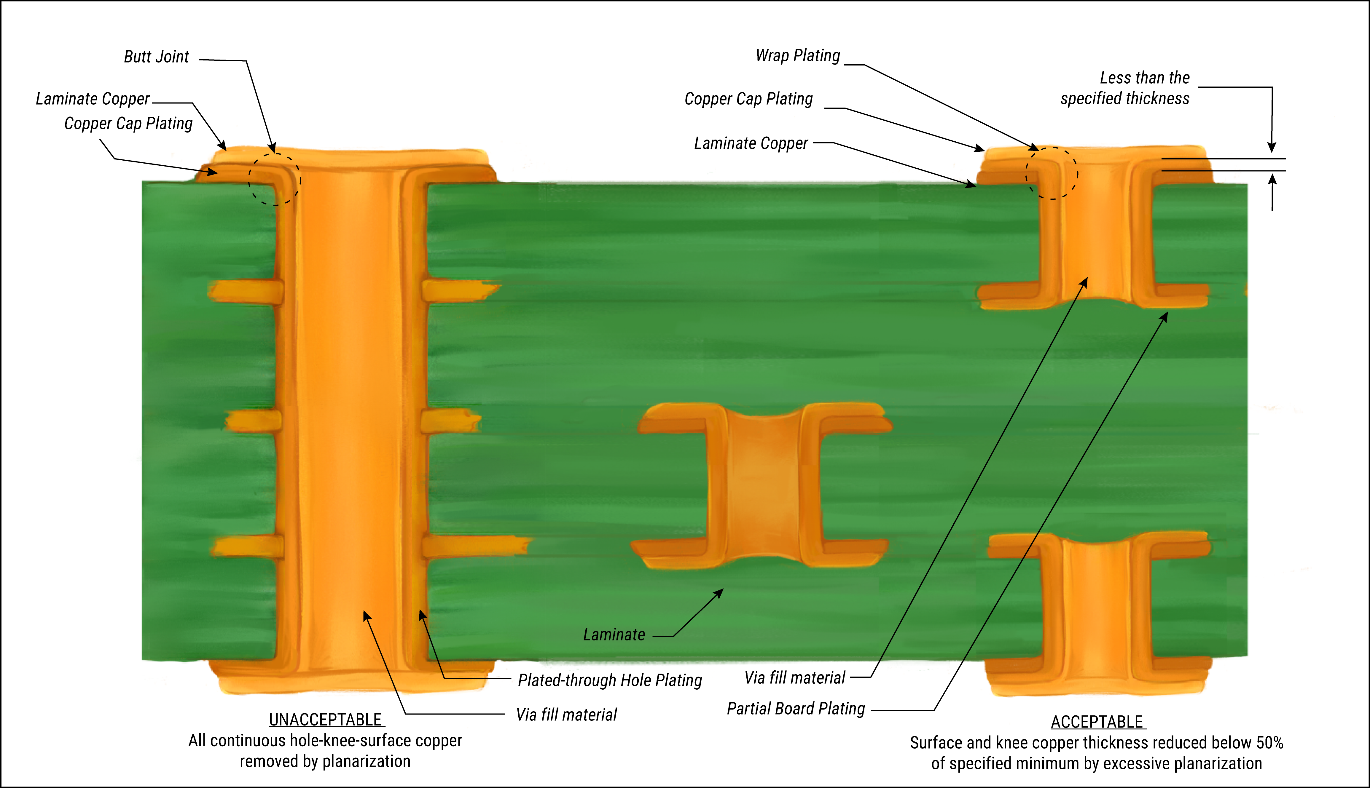
Outer layer copper thickness refers to the foil weight on the top and bottom surfaces of a PCB, typically expressed in ounces per square foot, which translates to specific micrometer thicknesses. Standard options range from lighter foils for signal layers to heavier ones for power distribution, directly affecting how vias interface with the board. In PCB via design, thicker outer copper enhances current handling on surface traces but requires careful via sizing to maintain plating uniformity during fabrication. Thicker foils demand larger annular rings around vias to accommodate etching tolerances and prevent breakout. IPC-6012 outlines performance specifications for rigid printed boards, including minimum copper plating thicknesses in vias to ensure wrap plating and barrel integrity. Proper selection prevents issues like via barrel cracking, especially in multilayer boards with high aspect ratios.
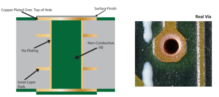
Vias serve as vertical interconnects, with types including through-hole, blind, and buried, each interacting differently with outer copper. Thicker outer layers can increase mechanical stress on via barrels during thermal cycling, as differential expansion occurs between the copper foil and plated via walls. Engineers must consider the copper thickness when defining via drill diameters and land sizes to avoid weakening the outer layers. This structured approach to PCB interconnect design supports signal integrity and power delivery across the stackup. Balancing these elements ensures vias contribute to overall board reliability without compromising routability.
Factors Affecting Copper Thickness and Via Reliability
Several factors govern copper thickness and via reliability, starting with plating thickness inside the via barrel. Industry standards mandate a minimum electroless and electrolytic copper plating to achieve sufficient conductivity and adhesion, typically targeting one mil or more for high-reliability applications. Thicker outer copper foils complicate plating distribution, as current density favors outer surfaces during electroplating, potentially thinning barrel walls at the center. Aspect ratio, defined as board thickness to via diameter, should stay below 10:1 to promote uniform deposition and void-free barrels. Material properties, such as dielectric constant and CTE mismatch, further influence reliability under thermal stress.
Mechanical reliability hinges on wrap plating, where copper extends over the via knuckle to anchor it to the surface foil. IPC-6012 specifies qualification tests like thermal shock and cross-section analysis to verify these features. Electromigration accelerates in thin copper under high current densities, making outer thickness a key mitigator for via current capacity. Corrosion resistance improves with heavier plating, vital for harsh environments. Engineers evaluate these through design rules that scale via pads and anti-pads with copper weight, ensuring robust transitions from traces to vias.
Thermal expansion differences between copper and the laminate exacerbate reliability risks in thick copper designs. Finite element modeling helps predict stress concentrations at via interfaces. Fabrication variables, like panel plating versus pattern plating, affect outcomes, with outer copper influencing etch-back and sidewall profiles. Comprehensive design reviews incorporate these factors to align copper thickness with via demands.
Via Current Capacity: Integrating Copper Thickness
Via current capacity determines how much amperage a via can handle without excessive temperature rise, guided by standards like IPC-2152. This standard provides charts correlating via diameter, copper plating thickness, and allowable delta-T for external and internal vias. Thicker outer copper allows wider traces feeding the via, increasing overall path capacity, but the bottleneck often remains the plated barrel. Engineers calculate using cross-sectional area of the barrel copper, factoring in plating thickness typically around 25 micrometers or more. For high-current paths, multiple vias in parallel boost capacity while distributing heat.
IPC-2152 emphasizes empirical data over legacy formulas, accounting for board thickness, ambient conditions, and convection. Outer layer thickness indirectly aids by enabling heavier power planes that reduce via loading. Conservative designs limit current density to below 500 A/cm2, adjusting for plating uniformity. Simulations validate these, incorporating thermal vias for dissipation. PCB interconnect design thus treats vias as thermal resistors in series with traces.
Temperature rise profiles differ for outer versus inner vias, with surface ones benefiting from convection. Heavier outer copper acts as a heat spreader, lowering local hotspots. Design tools implement IPC-2152 curves to automate width and via sizing. Reliability improves when current capacity aligns with operational margins.
Thermal Vias: Enhancing Heat Dissipation with Copper Optimization
Thermal vias transfer heat from components to inner planes or the opposite side, crucial in power electronics. Clusters of small-diameter vias under thermal pads maximize density while minimizing board real estate. Copper thickness on outer layers should match inner planes for efficient spreading, avoiding bottlenecks at transitions. Uncovered thermal vias, free of solder mask, improve wetting and conductivity during assembly. Aspect ratios below 8:1 ensure plating quality, preventing voids that impede heat flow.
In PCB via design, thermal vias complement outer copper pours, forming a distributed heat path. Filled vias, with conductive epoxy or copper, offer superior performance over plated-only. Diameter selection balances thermal conductance with fabrication yield, favoring 0.3 mm or larger for consistency. J-STD-001 addresses assembly cleanliness around these features to prevent bridging. Integration with outer thick copper elevates junction-to-ambient thermal resistance.
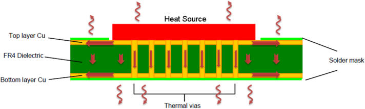
Heat flux calculations guide via count, using Fourier's law for conduction through barrel copper. Thicker plating enhances this path, synergizing with outer foil. Simulations predict performance under load, iterating designs for optimal theta-JA.
Best Practices for Reliable PCB Interconnect Design
Start with stackup planning, assigning heavier copper to outer layers for power and signals to inners. Define via rules scaling annular rings with foil weight, ensuring at least 0.15 mm for Class 3 boards per IPC guidelines. Use filled or tented vias for high-reliability to protect barrels. For via current capacity, consult IPC-2152 charts early, paralleling vias for redundancy. Incorporate thermal vias in power device footprints, spacing them 0.5-1 mm apart.
Fabrication drawings specify minimum plating thickness and wrap requirements. Simulate electromigration with current densities under worst-case loads. Prototype cross-sections verify plating uniformity. Maintain drill-to-copper clearances to prevent shorts during lamination. These practices yield interconnects resilient to vibration and cycling.
DFM reviews catch mismatches between copper thickness and via specs. Iterative testing with thermal cycling per IPC-6012 confirms reliability.
Troubleshooting Common Issues in Via and Copper Integration
Warpage from asymmetric copper thickness stresses vias, detectable via shadow moiré. Uneven plating signals high aspect ratios; downsize drills or thin stackups. Overheating vias indicate undersized barrels; recalculate per IPC-2152. Cracking at knuckles points to poor wrap; enhance plating cycles. Barrel pulls during rework suggest adhesion issues; check surface prep.
Systematic failure analysis uses dye-and-peel for microcracks. Adjust designs iteratively, prioritizing outer copper symmetry.
Conclusion
Outer layer copper thickness profoundly shapes PCB via design, dictating reliability, current capacity, and thermal performance. Best practices center on standards-driven rules for plating, sizing, and integration. Engineers achieve robust interconnects by balancing these with simulation and testing. Prioritizing copper thickness and via reliability ensures long-term system success. Adopt these strategies to elevate your PCB interconnect design.
FAQs
Q1: What role does outer layer copper thickness play in PCB via design?
A1: Outer layer copper thickness influences via reliability by affecting plating uniformity and mechanical anchoring. Thicker foils demand larger pads and better wrap plating to prevent cracking. IPC-6012 specifies minimums for performance. This ensures stable transitions in multilayer boards, supporting high-density layouts. Proper matching enhances overall PCB interconnect design.
Q2: How do you calculate via current capacity with varying copper thickness?
A2: Use IPC-2152 charts, inputting barrel plating thickness, diameter, and temperature rise limits. Thicker outer copper allows higher trace currents feeding the via. Account for external convection advantages. Multiple vias share load for safety margins. This method provides conservative ratings for copper thickness and via reliability.
Q3: Why are thermal vias essential in high-power PCB interconnect design?
A3: Thermal vias conduct heat from components through the stackup, preventing hotspots. Optimal designs use arrays with low aspect ratios and copper fill. Outer thick copper spreads heat effectively. Avoid solder mask plugs for better dissipation. They integrate seamlessly with power planes for reliable thermal management.
Q4: What are common pitfalls in copper thickness and via reliability?
A4: High aspect ratios lead to thin plating, risking electromigration. Asymmetric foils cause warpage stressing vias. Undersized annuli invite breakout. Mitigate with IPC-guided rules and simulations. Regular cross-sections verify compliance during prototyping.
References
IPC-6012F - Qualification and Performance Specification for Rigid Printed Boards. IPC, 2024
IPC-2152B - Standard for Determining Current Carrying Capacity in Printed Board Design. IPC, 2023
J-STD-001H - Requirements for Soldered Electrical and Electronic Assemblies. IPC, 2020


