Introduction
Solder wicking in via-in-pad designs poses a significant challenge for electrical engineers working on high-density printed circuit boards (PCBs). This phenomenon occurs when molten solder flows away from the intended pad area into the via during the reflow process, leading to weak or incomplete solder joints. Such defects can compromise the reliability of electronic assemblies, especially in compact designs like ball grid arrays (BGAs) and fine-pitch components. For engineers, understanding and preventing solder wicking is critical to ensuring robust connections and meeting stringent quality standards. This article explores the causes of solder wicking via-in-pad, its impact on PCB assembly, and practical techniques like via plugging, via tenting, and solder mask optimization to mitigate the issue. By implementing these solutions, engineers can enhance assembly outcomes and maintain design integrity.
What Is Solder Wicking in Via-in-Pad and Why It Matters
Solder wicking via-in-pad refers to the unintended migration of solder from a component pad into an adjacent via during the soldering process. This issue is prevalent in designs where vias are placed directly under or near component pads to save space in high-density layouts. While via-in-pad configurations optimize routing and reduce board size, they create a pathway for solder to escape, resulting in insufficient solder on the pad. This can lead to poor electrical connections, reduced mechanical strength, and potential failures in critical applications.
The significance of preventing solder wicking cannot be overstated. In industries like aerospace, automotive, and medical electronics, even minor defects can have severe consequences. Addressing this problem ensures consistent soldering quality, improves yield rates, and aligns with industry expectations for reliability. Engineers must prioritize strategies to control solder flow, especially in designs where space constraints demand via-in-pad placement.
Technical Principles Behind Solder Wicking in Via-in-Pad
Understanding the mechanisms of solder wicking via-in-pad begins with the behavior of molten solder during reflow. Solder naturally seeks the path of least resistance, driven by capillary action and surface tension. When a via is present near or under a pad, the open hole acts as a conduit, drawing solder away from the component joint. Several factors contribute to this issue.
First, the thermal dynamics of the reflow process play a role. Uneven heating can cause solder to melt and flow prematurely into vias before forming a proper joint on the pad. Second, the via’s surface finish, often copper with a thin plating, can attract solder more readily than the pad if not properly managed. Third, the absence of barriers like solder mask or plugs allows unrestricted solder movement into the via. Finally, the design of the stencil and the amount of solder paste applied can exacerbate the problem if excess paste is present near the via.
Standards such as IPC-4761 provide detailed guidelines on via protection types and their impact on solder flow. This standard categorizes methods like tenting, plugging, and filling, which directly address the risk of solder wicking. Engineers must consider these principles when designing layouts to minimize defects and ensure robust assembly processes.
Related Reading: Enhancing PCB Reliability with Via in Pad Technology
Causes of Solder Wicking in Via-in-Pad Designs
Several design and process-related factors contribute to solder wicking via-in-pad. Identifying these causes helps engineers implement targeted solutions.
-
Via Placement and Size: Placing vias directly under pads without protection increases the likelihood of solder escape. Larger via diameters can also draw more solder due to increased capillary action.
-
Lack of Via Protection: Open vias without tenting or plugging provide a direct path for solder to flow away from the pad during reflow.
-
Solder Paste Overapplication: Excessive solder paste near vias can result in surplus molten solder, which migrates into unprotected holes.
-
Reflow Profile Issues: Incorrect temperature profiles may cause uneven melting, allowing solder to flow into vias before forming a proper joint.
-
Surface Finish Compatibility: Certain finishes on vias and pads may promote solder wetting in undesirable areas, pulling solder away from intended joints.
Addressing these causes requires a combination of design adjustments and process controls, guided by standards like IPC-A-610, which outlines acceptability criteria for solder joints in electronic assemblies.
Related Reading: Troubleshooting Common Via-in-Pad Issues in PCB Design
Practical Solutions for Preventing Solder Wicking
Preventing solder wicking via-in-pad demands a multi-faceted approach, combining design techniques with assembly process optimizations. Below are proven strategies that electrical engineers can apply to mitigate this issue.
Via Plugging for Enhanced Protection
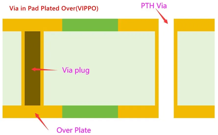
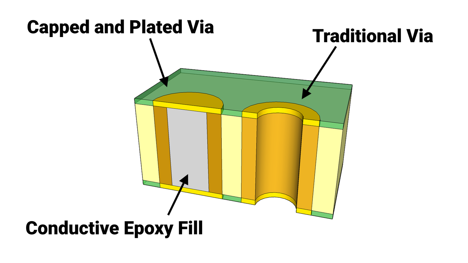
Via plugging involves filling the via with a non-conductive or conductive material to block solder flow. Non-conductive epoxy filling, as described in IPC-4761, prevents solder from entering the via while maintaining structural integrity. This method is particularly effective for high-density designs with BGAs, where vias under pads are common. Plugging ensures that solder remains on the pad, forming a reliable joint. Engineers should specify the filling material and process during design to ensure compatibility with thermal and mechanical requirements.
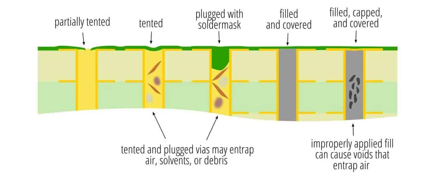
Via Tenting with Solder Mask
Via tenting uses a layer of solder mask to cover the via opening, creating a barrier against solder migration. According to IPC-4761, tenting can be applied on one or both sides of the PCB, depending on the design needs. This technique is cost-effective for less complex boards and prevents solder wicking via-in-pad by sealing the via entrance. However, engineers must ensure the solder mask adheres properly to avoid cracks or breaches during reflow, which could still allow solder to escape.
Optimized Solder Mask Design
Solder mask plays a critical role in controlling solder flow. Defining precise solder mask openings around pads and vias minimizes the risk of excess solder reaching unprotected areas. Standards like IPC-SM-840 provide guidelines for solder mask application and performance, ensuring durability under thermal stress. Engineers should design masks to cover via edges while leaving sufficient pad area for soldering. This balance prevents wicking while maintaining joint quality.
Stencil Design and Solder Paste Control
Adjusting stencil apertures to reduce solder paste near vias is another effective method. By limiting paste volume, engineers can prevent excess solder from flowing into unprotected vias. Additionally, aligning the reflow profile with recommendations from IPC-J-STD-020 ensures even heating and proper solder solidification. Careful control of paste application and thermal cycles reduces the likelihood of wicking during assembly.
Process Monitoring and Inspection
Post-assembly inspection, guided by IPC-A-600, helps detect solder wicking early. Visual checks and automated optical inspection can identify incomplete joints or solder in vias. Engineers should also monitor reflow oven settings to maintain consistent temperatures, preventing uneven solder flow. Regular process audits ensure adherence to design specifications and industry standards.
Troubleshooting Solder Wicking Issues in Assembly
When solder wicking via-in-pad occurs despite preventive measures, troubleshooting becomes essential. Engineers should start by reviewing the PCB design files to confirm via protection methods like plugging or tenting were correctly specified. Next, examining the reflow profile ensures temperatures align with component and material tolerances, as outlined in IPC-J-STD-020. If excess solder paste is suspected, reducing stencil aperture size near vias can help. Additionally, cross-sectional analysis of affected boards can reveal whether solder mask integrity or via filling failed during processing. Addressing these issues often requires collaboration between design and assembly teams to refine both layout and process parameters.
Conclusion
Solder wicking via-in-pad remains a persistent challenge in high-density PCB designs, but with the right techniques, electrical engineers can effectively mitigate its impact. By understanding the causes, such as unprotected vias and improper reflow conditions, and applying solutions like via plugging, via tenting, and optimized solder mask design, reliable solder joints become achievable. Standards from IPC provide a robust framework for implementing these strategies, ensuring consistency and quality. Through careful design and process control, engineers can overcome solder wicking, enhancing the performance and longevity of electronic assemblies in demanding applications.
FAQs
Q1: What causes solder wicking via-in-pad in PCB assembly?
A1: Solder wicking via-in-pad happens when molten solder flows into vias instead of forming a joint on the pad. This is often due to unprotected vias, excess solder paste, or uneven reflow temperatures. Design flaws like improper via placement also contribute. Following guidelines from industry standards helps identify and address these issues during the design phase.
Q2: How does via plugging help in preventing solder wicking?
A2: Via plugging fills the via with a material like epoxy, blocking solder from entering during reflow. As outlined in IPC-4761, this method ensures solder stays on the pad, forming strong joints. It is especially useful in high-density designs with vias under components, reducing the risk of weak connections.
Q3: What role does solder mask play in via tenting for preventing solder wicking?
A3: Solder mask in via tenting covers the via opening, acting as a barrier to solder flow. Per IPC-4761, this technique prevents solder wicking via-in-pad by sealing the via. Proper application ensures the mask withstands thermal stress, maintaining protection during assembly for reliable soldering outcomes.
Q4: How can engineers optimize designs to avoid solder wicking via-in-pad?
A4: Engineers can prevent solder wicking by using via plugging or tenting, refining solder mask layouts, and controlling solder paste volume. Adhering to standards like IPC-A-610 for joint quality and IPC-SM-840 for mask performance ensures effective design. Careful reflow profiling also minimizes solder migration risks.
References
IPC-4761 — Design Guide for Protection of Printed Board Via Structures. IPC, 2006.
IPC-A-610H — Acceptability of Electronic Assemblies. IPC, 2020.
IPC-A-600K — Acceptability of Printed Boards. IPC, 2020.
IPC-SM-840E — Qualification and Performance of Permanent Solder Mask and Flexible Cover Materials. IPC, 2010.
IPC-J-STD-020E — Moisture/Reflow Sensitivity Classification for Nonhermetic Surface Mount Devices. IPC, 2014.


