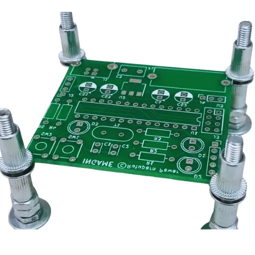
Mastering PCB Form Factor and Mounting Techniques for Reliable Designs
A comprehensive guide to PCB form factor, mounting hardware, enclosure design, and vibration-resistant techniques to ensure durable and optimized electronic assemblies.
Printed circuit boards (PCBs) form the backbone of modern electronics, enabling everything from smartphones to industrial machinery. In our PCB Knowledge category, we delve into the essential principles, techniques, and innovations that drive this field forward. Whether you are an engineer refining your designs or a hobbyist embarking on your first project, this collection offers valuable resources to enhance your understanding and skills. The scope of PCB Knowledge spans foundational concepts such as circuit layout and component selection, extending to advanced topics like high-speed signal integrity and thermal management. We provide detailed guides that walk through design software usage, manufacturing processes, and quality assurance methods. Tutorials offer hands-on instructions for prototyping and assembly, while insights from industry experts share real-world case studies and emerging trends. Best practices emphasize reliability, cost efficiency, and compliance with standards like IPC, ensuring your projects meet professional benchmarks. The practical value lies in its direct applicability to everyday challenges. For instance, articles on troubleshooting common PCB failures can save time and resources in product development cycles. Discussions on materials science reveal how choices in substrates and coatings impact performance in harsh environments, such as automotive or aerospace applications. By addressing these elements, PCB Knowledge equips you with tools to innovate and optimize electronic systems that power renewable energy solutions, medical devices, and consumer gadgets. As you read through the articles here, you will gain a comprehensive perspective that connects theoretical knowledge with tangible outcomes. This category serves as a hub for ongoing learning, where each piece builds on the others to foster expertise in PCB technology. Stay informed on the latest advancements, from flexible PCBs to sustainable manufacturing, and apply these insights to your work for superior results.
A comprehensive guide to PCB form factor, mounting hardware, enclosure design, and vibration-resistant techniques to ensure durable and optimized electronic assemblies.
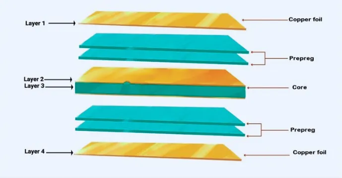
Explore the critical differences between symmetrical and asymmetrical PCB stackups, weighing their impact on performance, manufacturability, and cost to inform your circuit board design choices.
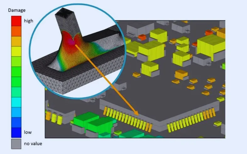
Electrical engineers can master solder joint fatigue life prediction, prevent failures, and enhance reliability by understanding thermal and vibration stress, FEA, and testing methods.
Learn how to design effective PCB silkscreen layers for better assembly, testing, and maintenance. This guide covers legibility, industry standards, and practical optimization tips.
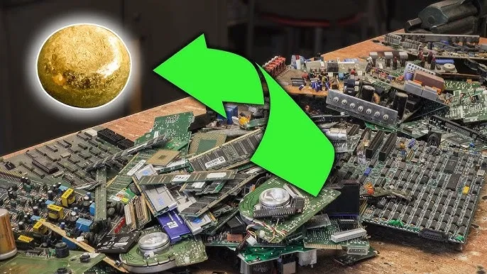
Learn safe DIY PCB recycling methods to extract copper and recover gold from e-waste. This guide details mechanical and chemical processes for recycling circuit boards at home.
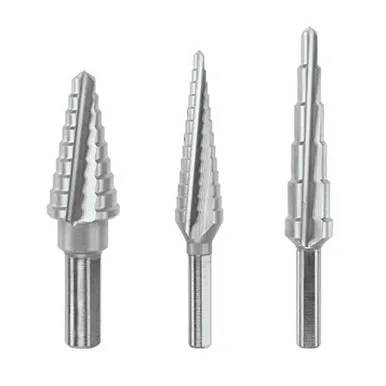
A comprehensive guide for engineers on choosing PCB drill bits, covering material types (carbide vs. HSS), sizes, and applications for FR-4 and microvias to ensure precise fabrication.
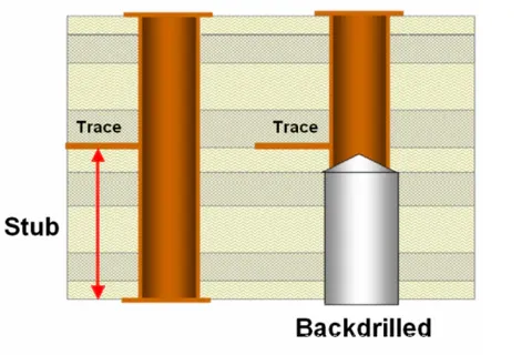
Master controlled depth drilling for better DIY PCB signal integrity. This guide offers practical tips and back drilling basics to enhance your home PCB projects.
Learn essential techniques for 50 ohm impedance control in PCB stackup design, covering microstrip and stripline calculations, material selection, and best practices for high-frequency applications.
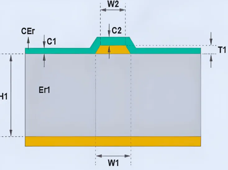
Discover the critical relationship between PCB trace width and impedance in high-speed designs. Learn how to calculate trace width for desired impedance and optimize signal integrity.
Learn how to determine the minimum PCB trace width for 20A currents using IPC-2221 standards, considering copper thickness, temperature rise, and layer placement.
Explore the critical role of PCB dielectric thickness in signal integrity, impedance control, and high-speed design, including FR-4 standards and calculation methods.
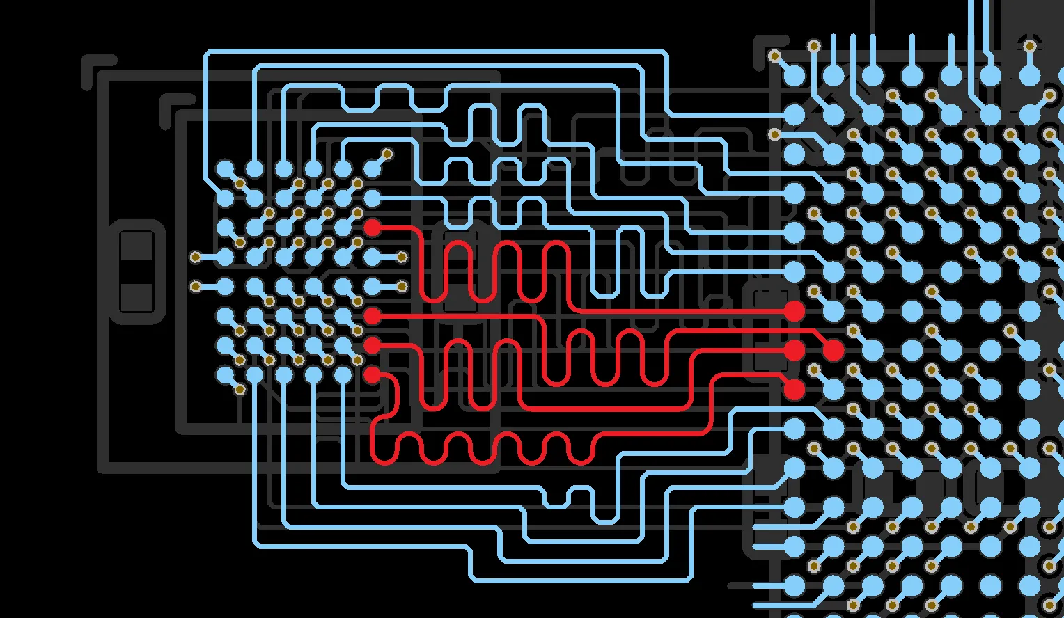
Learn how strategic placement, current capacity, and inductance management of power plane vias are crucial for robust PCB signal integrity.