Introduction
Six-layer printed circuit boards support complex electronics in compact forms. These boards integrate multiple signal and power layers for enhanced performance. As demands grow in sectors like telecommunications and computing, 6-layer PCB trends evolve rapidly. Innovations in materials and design address miniaturization needs. Future technology in 6-layer PCBs promises better signal integrity and efficiency.
This article examines key developments. It covers advanced materials, high-density interconnects, and embedded components. Engineers benefit from understanding these shifts to optimize designs. Procurement teams gain insights for reliable sourcing. AIVON provides guidance on aligning projects with emerging standards. Explore how these elements shape reliable assemblies.

What Is a 6-Layer PCB and Why It Matters
A 6 layer broad consists of six conductive layers separated by insulating dielectrics. It includes signal routing, ground planes, and power distribution. This configuration handles higher data rates than simpler boards. Standards like IPC-2221B outline design parameters for multilayer boards.
These PCBs matter in modern applications. They support 5G networks and Internet of Things devices. Increased layer count reduces crosstalk and improves electromagnetic compatibility. In automotive electronics, 6-layer boards manage sensor data flows. As devices shrink, these boards enable dense component placement.
Future relevance stems from performance demands. High-speed interfaces require controlled impedance. 6-layer PCB future technology integrates with artificial intelligence systems. Boards must withstand thermal cycles while maintaining flatness. Compliance with IPC-6012E ensures qualification for rigid multilayer use. Designers select these for balanced cost and capability.
Key Trends Shaping 6-Layer PCB Technology
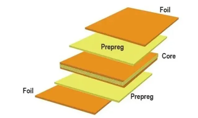
Trends in 6-layer PCB technology focus on density and sustainability. Miniaturization drives adoption in consumer gadgets. Higher layer counts accommodate finer traces. Sequential lamination builds allow microvia integration.
Advanced Materials for Enhanced Performance
Advanced materials elevate 6-layer PCB advanced materials usage. Low-loss dielectrics reduce signal attenuation at gigahertz frequencies. High glass transition temperature resins withstand reflow peaks. IPC-4101F specifies base materials for rigid boards, including halogen-free options.
Developers favor polyimide for flexibility in rigid-flex hybrids. These materials offer thermal stability up to 260°C. Ceramic-filled composites improve heat dissipation in power sections. Sustainability pushes for recycled content without compromising dielectric constants.
Selection depends on application. For RF modules, low coefficient of thermal expansion matches components. Factory processes verify material uniformity per IPC-TM-650 2.5.5. These choices extend board life in harsh environments.
The table below compares popular options in 2026:
| Material | Dk | Tg (°C) | CTE (ppm/°C) | Key Benefit | Relative Cost |
|---|---|---|---|---|---|
| Rogers RO4000 Series | 3.38 | >280 | 11-13 | Excellent RF performance, low loss | High |
| Panasonic Megtron 7 | 3.4 | >200 | Low | Balanced high-speed & thermal stability | Medium-High |
| I-Tera MT40 | 3.45 | ~200 | 12 | Cost-effective for high-volume AI servers | Medium |
These advanced low-loss materials extend board life in harsh automotive and aerospace environments while reducing overall material waste by up to 20% when optimized with AI tool

High-Density Interconnect Integration
High-density interconnect transforms 6-layer PCB high-density interconnect capabilities. HDI employs blind and buried vias for tighter routing. Microvias under 150 microns enable component proximity. IPC-6016D qualifies HDI PCBs for dense builds.
This trend supports ball grid array footprints. Stacked vias connect layers efficiently. Aspect ratios reach 1:1 for laser-drilled holes. Design rules limit via stubs to minimize reflections. Simulations predict eye diagrams for compliance.
In production, sequential buildup adds layers incrementally. This method controls registration accuracy. HDI reduces board size by 30% in compact devices. Applications include wearables and medical implants.
Embedded Components for Compact Designs
Embedded components redefine space usage in 6-layer PCB embedded components. Resistors and capacitors integrate into dielectrics. This approach frees surface area for active devices. IPC-7095D provides guidelines for embedded passives.
Polymer thick film prints circuits directly on layers. Capacitors form between power and ground planes. Inductors embed in magnetic cores for filters. Assembly skips surface mount for these elements.
Benefits include shorter loops for noise reduction. Thermal management improves as heat spreads evenly. Challenges involve precise placement during lamination. Test methods per IPC-TM-650 2.6.7 verify functionality post-process.

Suggested Reading: Designing a 6-Layer PCB for EMI/EMC Compliance: A Comprehensive Guide
Innovations Driving the Future of 6-Layer PCBs
Innovations propel 6-layer PCBs toward smarter manufacturing. Additive processes like 3D printing prototype complex geometries. Aerosol jet deposition patterns conductive inks on curved surfaces.
Artificial intelligence optimizes stackups. Algorithms predict warpage from material properties. This reduces iterations in design cycles. Standards like IPC-2581C standardize digital data exchange for AI tools.
Suggested Reading: 6-Layer PCB Stackup for Power Electronics: Design for High Current and Voltage
Flexible substrates blend with rigid sections for foldable electronics. Semi-flex designs route signals across bends. Power integrity tools simulate plane splits to avoid voltage drops.
Sustainability innovations include lead-free finishes and low-energy cures. Recyclable laminates lower environmental impact. Factories adopt closed-loop water systems for etching.
These advances align with ISO 14001 for environmental management. Procurement benefits from traceable supply chains. AIVON supports clients in selecting verified materials.
Industry Applications and Real-World Case Studies
In 5G networking equipment, 6-layer boards with dedicated ground planes successfully manage 100G+ Ethernet signals while meeting stringent FCC emissions requirements. Automotive ADAS systems leverage HDI and embedded components to process sensor data with low latency, achieving up to 40% size reduction in control modules and improving thermal performance in harsh under-hood environments.
Medical portable diagnostics benefit from embedded passives that reduce battery drain and overall device weight. In edge AI computing, balanced stackups ensure thermal uniformity during machine learning inference tasks. One notable case study involves an IoT gateway manufacturer that switched to optimized 6-layer HDI designs, cutting board size by 35% while improving signal integrity and passing all EMC testing on the first revision.
Design, Manufacturing Considerations, and Cost Trends
Successful implementation requires early design-for-manufacturability (DFM) reviews, careful material selection, and simulation of power integrity and thermal behavior. In 2026, the cost premium for a well-designed 6-layer board is typically 1.5–1.8× that of a 4-layer equivalent, but the ROI is compelling due to higher density, fewer assemblies, and reduced field failures.
Markdown ROI Comparison Table:
| Configuration | Routing Density | Relative Cost | Typical ROI Payback (High-Volume) | Best For |
|---|---|---|---|---|
| 4-Layer | Baseline | 1.0× | 12–18 months | Simple designs |
| 6-Layer | 2.5× | 1.6× | 6–9 months | High-speed, compact AI/5G |
| 8-Layer | 4× | 2.4× | 9–14 months | Ultra-complex systems |
Challenges, Solutions, and Implementation Roadmap for 2026
Key challenges include layer registration accuracy in HDI builds, warpage in thin constructions, rising material costs, and increasing complexity of signal integrity requirements. Solutions center on AI predictive modeling, improved laser drilling equipment, and tighter supply-chain collaboration with verified material suppliers.
A practical 2026 implementation roadmap includes: (1) Define electrical and thermal requirements early, (2) Use AI-assisted stackup tools for initial design, (3) Validate with simulation and prototype runs, (4) Conduct thorough DFM reviews with your fabrication partner, and (5) Scale production while monitoring sustainability metrics. Starting with a trusted manufacturer helps mitigate risks and compress the overall timeline.
Conclusion
The future of 6-layer PCBs blends density with efficiency. Trends in advanced materials and HDI meet rising demands. Embedded components enable sleeker profiles. Innovations like AI design streamline development.
Adopt these for competitive edges in electronics. Standards guide reliable outcomes. AIVON offers expertise in navigating these shifts. Stay informed to future-proof projects.
FAQs
Q1: What are the main 6-layer PCB trends for 2025?
A1: 6-layer PCB trends emphasize miniaturization and high-speed support. HDI vias enable denser routing. Sustainability drives halogen-free materials. AI tools optimize layouts for signal integrity. These align with applications in 5G and AI devices.
Q2: How do advanced materials impact 6-layer PCB future technology?
A2: Advanced materials in 6-layer PCB future technology lower losses and boost thermal performance. Low-Dk dielectrics suit RF signals. High-Tg resins endure assembly heats. IPC-4101F ensures material specs. Selection enhances reliability in compact builds.
Q3: Why integrate high-density interconnect in 6-layer PCBs?
A3: High-density interconnect in 6-layer PCBs packs more functions into small spaces. Microvias reduce trace lengths. This cuts crosstalk in high-speed designs. IPC-6016D sets performance benchmarks. It supports BGA components effectively.
Q4: What benefits come from 6-layer PCB embedded components?
A4: 6-layer PCB embedded components save surface space and shorten signal paths. Passives integrate seamlessly for noise control. This improves power efficiency. IPC-7095D outlines design rules. Applications gain from compact, reliable assemblies.
References
IPC-2221B — Generic Standard on Printed Board Design. IPC, 2009.
IPC-6012E — Qualification and Performance Specification for Rigid Printed Boards. IPC, 2017.
IPC-4101F — Specification for Base Materials for Rigid and Multilayer Printed Boards. IPC, 2017.
IPC-6016D — Qualification and Performance Specification for High Density Interconnect (HDI) Printed Boards. IPC, 2018.
IPC-7095D — Design and Assembly Process Implementation for Embedded Components. IPC, 2019.
IPC-TM-650 — Test Methods Manual. IPC, various revisions.
IPC-2581C — Printed Board/Printed Component Information and Traceability Specification. IPC, 2020.
ISO 14001:2015 — Environmental Management Systems. ISO, 2015.