Introduction
Selecting the right panel size for a PCB prototype is a critical decision for electrical engineers working on new designs. The panel size directly influences manufacturing efficiency, cost, and the quality of the final prototype. For low volume production or initial testing phases, the choice of PCB prototype panel size can impact turnaround time and material usage. This article explores key considerations for determining the optimal panel size for prototype PCBs, focusing on technical constraints, industry standards, and practical guidelines. Whether you are designing for a small batch or planning for future scalability, understanding panel size for prototype PCB projects ensures smoother workflows and better outcomes. Let’s dive into the factors that shape this decision for engineers.
What Is PCB Panel Size and Why It Matters
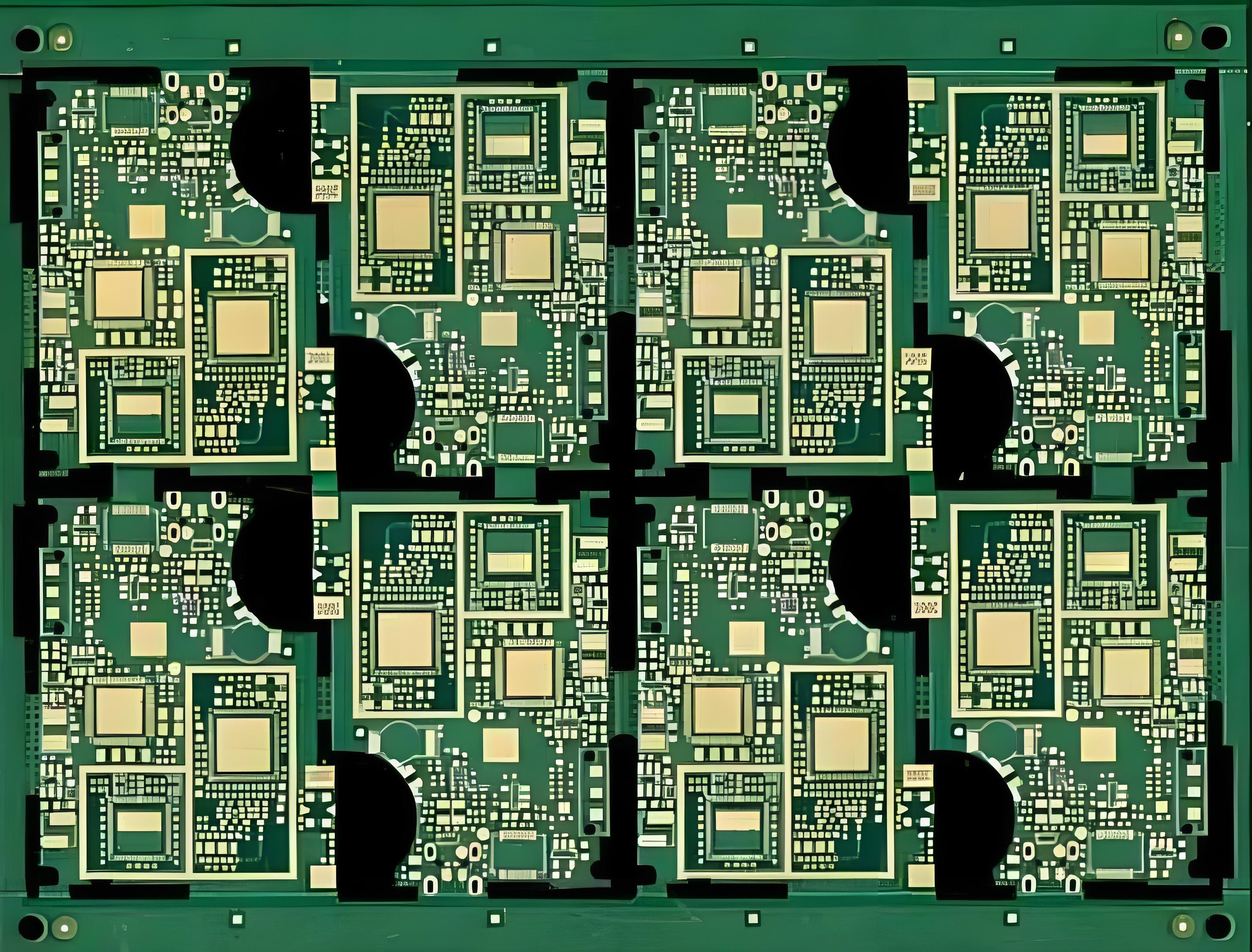
PCB panel size refers to the dimensions of the larger board that holds multiple individual PCB designs during manufacturing. In prototype development, panelization allows several identical or different boards to be fabricated and assembled together before being separated into individual units. This process is essential for efficiency, especially in PCB panel low volume production where costs per unit can be high.
The importance of panel size lies in its effect on manufacturing processes. A well chosen panel size reduces waste, optimizes machine utilization, and minimizes handling errors. For electrical engineers, it also affects testing and assembly timelines. If the panel is too small, production may become inefficient. If too large, it risks exceeding equipment limits or increasing material costs. Balancing these factors ensures that the panel size for prototype PCB aligns with project goals and budget constraints.
Technical Principles Behind PCB Panel Size Selection
Equipment and Process Limitations
Manufacturing facilities have specific constraints on the maximum and minimum panel sizes their equipment can handle. Most standard fabrication lines accommodate panel sizes ranging from small formats for prototypes to larger ones for mass production. Electrical engineers must consider the capabilities of the fabrication house to avoid compatibility issues. For instance, exceeding the maximum panel size can lead to processing delays or the need for custom setups, which increase costs.
Material Utilization and Waste Reduction
Panel size directly impacts how much raw material is used. Larger panels can accommodate more individual boards, reducing waste per unit. However, for low volume runs like PCB panel low volume projects, oversized panels may result in unused space, driving up costs. Engineers should aim to maximize the number of boards per panel while adhering to design spacing rules to prevent issues during depanelization.
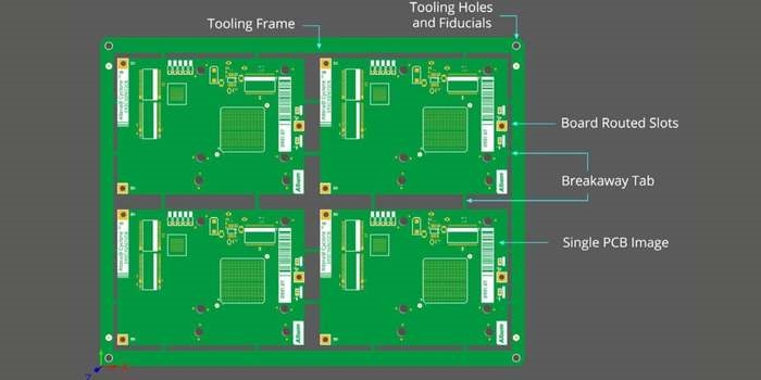
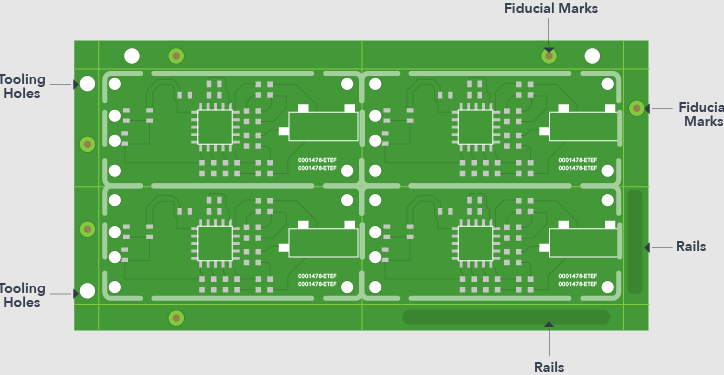
Depanelization and Breakout Methods
Depanelization, the process of separating individual PCBs from the panel, is influenced by panel size and layout. Common methods include scoring, routing, and punching. The chosen method must align with the panel size to ensure clean separation without damaging components or traces. For prototype PCBs, engineers often prefer routing for precision, which requires adequate spacing around each board. This spacing must be factored into the overall panel size for prototype PCB designs.
Compliance with Industry Standards
Adhering to recognized standards ensures manufacturability and quality. For instance, IPC-2221B, a widely accepted guideline for PCB design, provides recommendations on panelization and spacing to avoid mechanical stress during fabrication and assembly. Following such standards helps engineers select a panel size that supports structural integrity and minimizes risks like warpage or cracking during processing.
Practical Guidelines for Choosing the Best Panel Size
Assess Project Volume and Goals
For PCB panel low volume runs, smaller panel sizes are often more cost effective. If the project involves only a few prototypes for testing, a compact panel reduces material costs and simplifies handling. Conversely, if the prototype phase might scale to small batch production, consider a slightly larger panel size to test manufacturing consistency. Aligning panel size with the project’s immediate and future needs prevents redesign efforts later.
Optimize Board Layout for Efficiency
Arrange individual PCB designs on the panel to maximize space utilization. Use nesting techniques to fit as many boards as possible while maintaining necessary clearances for depanelization. Software tools adhering to industry standards like IPC-6012E can assist in simulating panel layouts to identify the most efficient configuration. This step is crucial for PCB prototype panel size decisions, especially in low volume scenarios.
Consider Assembly and Testing Requirements
Panel size affects not only fabrication but also assembly and testing phases. Larger panels can streamline automated assembly by reducing the number of setups. However, for manual testing or inspection common in prototypes, smaller panels may be easier to handle. Ensure the chosen panel size for prototype PCB accommodates fiducial marks and test points without overcrowding, as recommended by guidelines in IPC-A-600K.
Account for Material and Thickness Constraints
The thickness and type of substrate material influence panel size feasibility. Thicker boards or those with specialized materials may have restrictions on maximum panel dimensions due to handling or processing limitations. Consult fabrication guidelines to confirm that the selected panel size aligns with material properties, preventing issues like excessive warpage during thermal cycles.
Related Reading: Panel Design for Manufacturing: A Comprehensive Overview
Plan for Scalability and Future Production
Even in prototype stages, consider how panel size might affect transition to higher volume production. A panel size that works for a few units may not be optimal for hundreds. Standardizing panel dimensions early, in line with common manufacturing formats, can simplify scaling. This foresight is particularly valuable for PCB panel low volume projects aiming for eventual mass production.
Common Challenges and Troubleshooting Tips
Misalignment with Fabrication Capabilities
A frequent issue is selecting a panel size incompatible with the manufacturer’s equipment. To avoid this, request fabrication constraints upfront and cross reference them with design plans. If a custom panel size is unavoidable, allocate additional time for setup and validation to ensure compliance with standards like IPC-6012E.
Excessive Material Waste
Poor panel utilization leads to higher costs, especially in PCB panel low volume runs. Use layout optimization tools to test different arrangements before finalizing the design. Aim for minimal unused space while maintaining clearances for breakout tabs or routing paths as per IPC-2221B guidelines.
Handling and Assembly Errors
Oversized panels can be cumbersome during manual handling or testing, increasing the risk of damage. If large panels are necessary, incorporate handling edges or rails as recommended by IPC-A-600K. For smaller runs, prioritize manageable panel sizes to reduce error rates during prototype validation.
Related Reading: Troubleshooting PCB Panelization: Common Problems and Expert Solutions
Conclusion
Selecting the best panel size for a PCB prototype is a multifaceted decision that balances manufacturing efficiency, cost, and design requirements. By understanding equipment limitations, optimizing layouts, and adhering to industry standards like IPC-2221B and IPC-6012E, electrical engineers can make informed choices for PCB prototype panel size. Practical considerations, such as project volume and future scalability, further refine this process. Whether working on PCB panel low volume runs or preparing for production, a strategic approach to panel size ensures smoother prototyping and reliable outcomes. Careful planning at this stage lays the foundation for successful PCB development.
FAQs
Q1: What factors influence the choice of PCB prototype panel size?
A1: The choice of PCB prototype panel size depends on manufacturing equipment limits, material utilization, and project volume. Design layout, depanelization methods, and assembly needs also play a role. Standards like IPC-2221B guide spacing and structural integrity. Engineers must balance cost efficiency with manufacturability to select an optimal size for prototype testing.
Q2: How does panel size affect PCB panel low volume production costs?
A2: Panel size impacts PCB panel low volume production costs through material usage and processing efficiency. Smaller panels reduce waste for limited runs but may increase per unit handling time. Larger panels can lower costs per board if space is utilized well, but unused areas raise expenses. Optimizing layout is key to cost control.
Q3: What is the ideal panel size for a prototype PCB project?
A3: The ideal panel size for a prototype PCB varies based on design count and manufacturer constraints. For small runs, compact panels minimize material costs. Larger panels suit projects with multiple boards or future scaling. Referencing IPC-6012E ensures compatibility with fabrication processes, tailoring the size to specific project needs.
Q4: How can engineers optimize panel size for prototype PCB designs?
A4: Engineers can optimize panel size for prototype PCB by maximizing board count per panel through efficient nesting. Maintain clearances for depanelization as per IPC-A-600K. Assess assembly and testing needs to avoid handling issues. Aligning with fabrication limits and planning for scalability ensures the chosen size supports both current and future goals.
References
IPC-2221B — Generic Standard on Printed Board Design. IPC, 2012.
IPC-6012E — Qualification and Performance Specification for Rigid Printed Boards. IPC, 2020.
IPC-A-600K — Acceptability of Printed Boards. IPC, 2020.


