Why is PCB Grounding Essential for Noise Reduction and Reliability?
Grounding in Printed Circuit Board (PCB) design forms the bedrock of stable electrical performance. A meticulously designed ground system effectively minimizes unwanted noise, prevents various forms of interference, and ensures that both signals and power are delivered dependably across the entire board. Inadequate grounding, conversely, can precipitate a host of issues, including electromagnetic interference (EMI), ground loops, and signal distortion, all of which can severely degrade a device's performance or even lead to its complete failure.
By implementing robust grounding techniques, designers can achieve substantial noise reduction, preserve signal integrity, and establish reliable connections among all components. Let’s delve into the fundamental principles and specific methodologies to accomplish these critical objectives.
What Are the Basic Principles of PCB Grounding?
Before delving into more advanced strategies, it's crucial to grasp the foundational concepts of PCB grounding. Grounding refers to the practice of connecting various parts of an electrical circuit to a common reference point—typically a ground plane or a designated ground trace. This connection provides a stable return path for electrical currents, which helps in maintaining consistent voltage levels and diminishing extraneous noise.
On a PCB, the ground serves multiple vital functions:
● Noise Suppression: It actively prevents interference by offering a low-impedance pathway for stray currents, directing them away from sensitive areas.
● Signal Integrity: It maintains stable reference voltages for signal lines, a particularly crucial aspect in high-speed circuit designs where timing and waveform quality are paramount.
● Safety Assurance: It safeguards both users and components by diverting fault currents safely away from sensitive parts of the circuit.
Without proper grounding, designers might encounter problems such as crosstalk between adjacent traces or unpredictable and erratic behavior within their circuits. Now, let’s explore specific techniques aimed at optimizing grounding for enhanced noise reduction and more reliable connections.
Key PCB Grounding Techniques for Effective Noise Reduction
Implementing a Dedicated Ground Plane
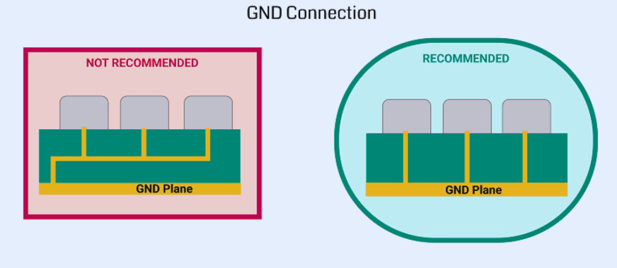
One of the most potent strategies for mitigating noise in a PCB is the integration of a dedicated ground plane. This is a large, continuous layer of copper on the PCB that functions as a universal ground reference for all components. It provides an exceptionally low-impedance path for return currents, thereby significantly minimizing noise and electromagnetic interference.
For instance, in a typical stack-up of the four layer PCB, it is common practice to dedicate one entire layer exclusively to grounding. This configuration can reduce EMI by as much as 20 dB compared to designs that rely solely on narrow ground traces. It is crucial to keep the ground plane as continuous and unbroken as possible; avoid splitting it with signal traces or vias unless absolutely unavoidable, as such breaks can create high-impedance pathways and consequently increase noise.
Minimizing Ground Loops
Ground loops arise when multiple distinct paths exist for ground currents to flow, leading to differences in electrical potential that can introduce unwanted noise. To circumvent ground loops, ensure that all components connect to a single, unified ground point or plane. This approach is particularly vital in mixed-signal designs, where sensitive analog signals and noisy digital signals coexist.
For example, if you are designing a board that incorporates both analog sensors and digital microcontrollers, it is advisable to separate the analog and digital ground planes. However, these separate planes should be connected at one single point, ideally near the power supply. This strategy prevents high-frequency digital switching noise, which can reach 100 MHz or higher, from corrupting sensitive analog signals.
Shortening Return Paths
Return paths are the routes that electrical currents take back to their source. Extended return paths increase impedance and can lead to both noise induction and signal delays. To minimize these adverse effects, components should be placed in close proximity to their ground connections. Furthermore, signal traces should be routed directly over the ground plane to ensure the return path is as short and direct as possible.
In high-speed designs, such as those operating at 1 GHz or more, an excessively long return path can introduce signal delays of several nanoseconds, potentially causing critical timing errors. Maintaining short return paths is fundamental for ensuring reliable connections and achieving superior noise reduction.
How Do Bypass Capacitors Enhance Noise Reduction?
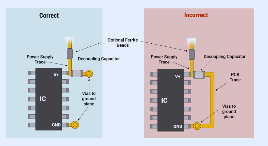
Bypass capacitors, also commonly referred to as decoupling capacitors, play a pivotal role in effective PCB grounding and noise reduction. These capacitors are strategically placed between the power supply and ground, in close proximity to active components like integrated circuits (ICs). Their primary function is to filter out high-frequency noise and stabilize voltage levels, especially during rapid current demands.
Here’s how to effectively deploy bypass capacitors:
● Optimal Placement: Position bypass capacitors as close as physically possible to the power pins of the ICs they are decoupling. An ideal distance is less than 0.1 inches (approximately 2.54 mm) to minimize parasitic inductance.
● Value Selection: Utilize a combination of capacitor values, typically 0.1 μF and 1 μF, to effectively filter a broad spectrum of frequencies. For example, a 0.1 μF capacitor is effective against noise up to around 100 MHz, while a larger 10 μF capacitor addresses lower-frequency fluctuations and power supply ripple.
● Ground Connection: Connect the capacitor directly to the ground plane using a short, wide via. This minimizes parasitic inductance in the connection, which could otherwise diminish the capacitor's filtering effectiveness.
By strategically incorporating bypass capacitors, designers can achieve substantial noise reduction, ensuring that the power supply remains stable even during fast switching events and transient loads.
Optimizing Power Supply Design with Grounding Techniques
The power supply section is another critical area where effective grounding techniques can significantly enhance overall reliability and reduce noise. A poorly designed power supply layout can introduce ripple and various forms of interference, negatively impacting the performance of the entire circuit.
Here are some best practices for integrating grounding with power supply design:
● Separate Power and Ground Planes: In multilayer PCBs, it is highly recommended to dedicate separate internal layers for power and ground planes. Placing these layers adjacent to each other creates a natural capacitance effect, which inherently helps to filter out high-frequency noise. For instance, in a 6-layer board, the ground plane might be on layer 2 and the power plane on layer 3, positioned closely for optimal coupling.
● Implementing Star Grounding for Power Distribution: Star grounding is a technique where all ground connections for a specific power domain converge at a single central node, typically located near the power supply input. This method is highly effective in preventing ground loops and ensures that noise generated in one part of the circuit does not propagate and affect other sensitive sections. It is particularly beneficial in designs featuring multiple power domains, such as a board with both 3.3V and 5V sections.
● Careful Power Trace Routing: When routing power traces, it is crucial to keep them short and wide to minimize both resistance and inductance. A trace width of 20 mils (0.5 mm) or more is generally recommended for power lines carrying currents of 1A or greater to minimize voltage drops. Furthermore, avoid routing power traces over any splits or discontinuities in the ground plane, as this can disrupt the return current paths and introduce undesirable noise.
By meticulously applying these power supply grounding techniques, designers can ensure robust, reliable connections and a consistently stable voltage supply, both of which are fundamental to the overall high performance of their PCB.
Grounding Strategies for Mixed-Signal and High-Speed Designs
Grounding for Mixed-Signal Boards
Mixed-signal PCBs, which integrate both analog and digital components, demand particular attention to grounding due to the potential for digital circuits to generate high-frequency noise that can interfere with sensitive analog signals.
To effectively manage this, adhere to the following guidelines:
● Separate Analog and Digital Grounds: Implement distinct ground planes for analog and digital sections to isolate noise effectively. Crucially, connect these separate planes at a single designated point, ideally located near the power supply entry point or the analog-to-digital converter (ADC), to prevent the formation of ground loops.
● Judicious Signal Routing: Maintain clear physical separation between digital traces and analog components. For example, a 50 MHz digital clock signal and its harmonics can easily couple into nearby analog traces, leading to erroneous measurements or system instability.
● Strategic Shielding: If physical separation is not entirely feasible, consider incorporating guard traces or dedicated shielding around sensitive analog areas, ensuring these are properly connected to the analog ground plane. These measures help to contain and divert electromagnetic interference.

Advanced Grounding for High-Speed PCBs
For high-speed designs, encompassing interfaces like USB, HDMI, or radio frequency (RF) signals, grounding becomes even more critically important.
Here are some advanced techniques to implement:
● Controlled Impedance Management: Ensure that the ground plane provides adequate support for controlled impedance traces, which are essential for maintaining signal integrity in high-speed applications. A typical 50-ohm impedance for RF signals, for instance, requires precise calculation of trace width and proximity to the ground plane, often facilitated by specialized PCB design software.
● Eliminate Ground Plane Gaps: Avoid any gaps, voids, or discontinuities in the ground plane directly beneath high-speed traces. Such interruptions can cause signal reflections and degrade waveform quality. The ground plane should remain continuous under these critical traces.
● Utilize Stitching Vias: In multilayer boards, employ stitching vias to effectively connect ground planes across different layers. This practice significantly reduces loop inductance and noise. Vias should be spaced at intervals approximately 1/8th of the wavelength of the highest signal frequency (e.g., every 3.75 mm for a 10 GHz signal).
These advanced grounding techniques are indispensable for preserving the integrity of high-speed signals, minimizing noise induction, and ensuring highly reliable connections throughout the PCB.
Common Grounding Mistakes and How to Avoid Them
Even with the best intentions, certain grounding errors can compromise the effectiveness of your PCB design.
Here are some prevalent pitfalls and strategies to avoid them:
● Unnecessary Ground Plane Splits: Fragmenting a ground plane without a clear, functional reason can inadvertently create high-impedance return paths, thereby increasing noise. Only split planes when it is necessary to separate analog and digital grounds, and always ensure these are connected at a single, well-defined point.
● Ignoring Via Placement: While vias are crucial for connecting components to the ground plane, placing them too far from the component pins increases parasitic inductance. Always use multiple vias for high-current paths to effectively reduce overall impedance.
● Neglecting Bypass Capacitors: Failing to incorporate bypass capacitors or placing them improperly can lead to significant power supply noise. It is imperative to always include these capacitors in close proximity to the power pins of all active integrated circuits.
By proactively recognizing and addressing these common mistakes, designers can create PCBs that exhibit superior noise reduction characteristics and feature more robust, reliable connections.
Conclusion: Effective PCB grounding is undeniably the cornerstone for minimizing noise and ensuring reliable connections within your electronic designs. By judiciously employing a dedicated ground plane, actively minimizing ground loops, strategically incorporating bypass capacitors, and meticulously optimizing power supply layouts, you can dramatically enhance the overall performance and stability of your circuits. Whether you are developing a straightforward prototype or an intricate high-speed board, these fundamental grounding techniques are crucial for achieving excellent noise reduction and maintaining impeccable signal integrity. Always remember to customize your grounding approach to align precisely with the specific requirements of your design, whether it involves mixed-signal functionalities or high-frequency applications. With meticulous planning and unwavering attention to detail, you possess the capability to engineer PCBs that consistently perform reliably under all operating conditions. We invite you to implement these proven PCB grounding techniques in your next project to experience a tangible improvement in both noise reduction and connection reliability. Your sophisticated designs will undoubtedly benefit from this dedicated attention to foundational principles.


